1994 Buick Century 3.1L lower intake manifold gasket replacement
This is a fairly involved job that requires some planning ahead of time.
This is a fairly involved job that requires some planning ahead of time.


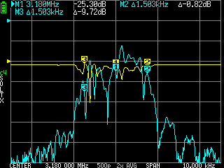
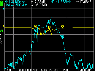
This happened after a heat gun was used to heat cycle the crystals three times. The rejection at marker 2 improved from about 1 dB to 7 dB.
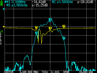
Next all the solder joints were reheated on the pcb. One solder joint to a 50 pF capacitor had a very strong effect bringing the rejection at marker 2 to nearly 18 dB.
If the crystals are heated momentarily, the response starts to improve to the point that it looks reasonable as shown below. Unfortunately it returns to the above image when it cools. There was also a significant decrease in the insertion loss.
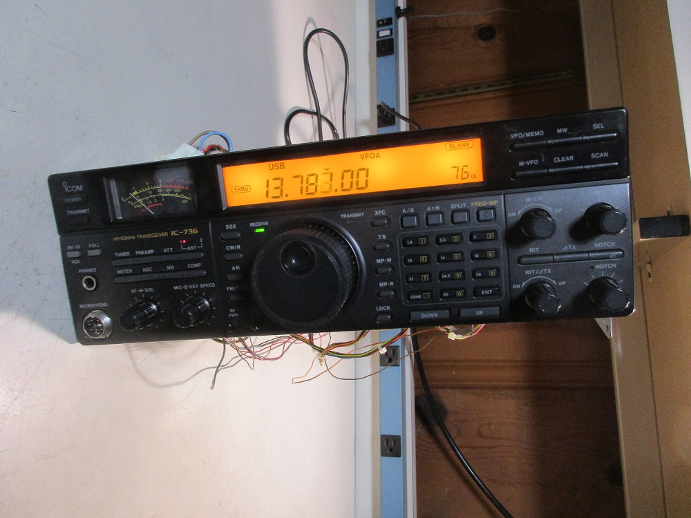
The Icom 736 is not a particularly well known transceiver. I had not heard of it before acquiring an Icom PW-1 amplifier where it was found that the 736 is required to complete the testing of the PW-1 tuner. For that reason, it came on the list of rigs to acquire. Recently, a 736 parts unit was found for a very good price. This is it’s story. The knobs have been taken off for cleaning. An attempt to turn it on resulted in no activity at all.
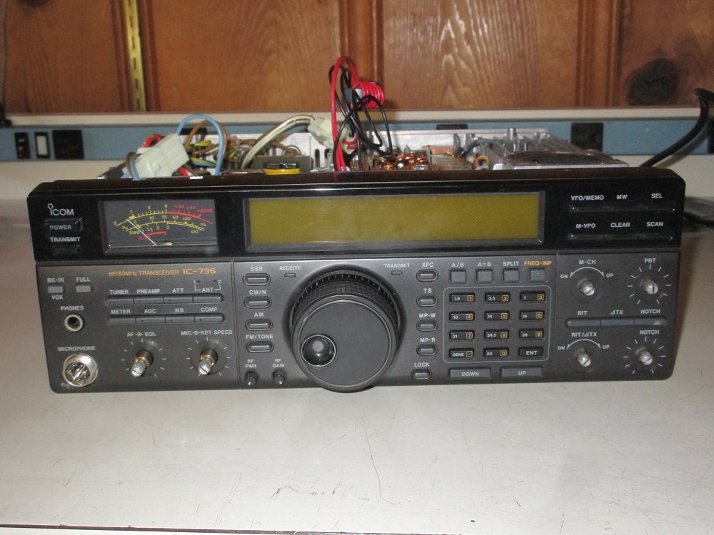
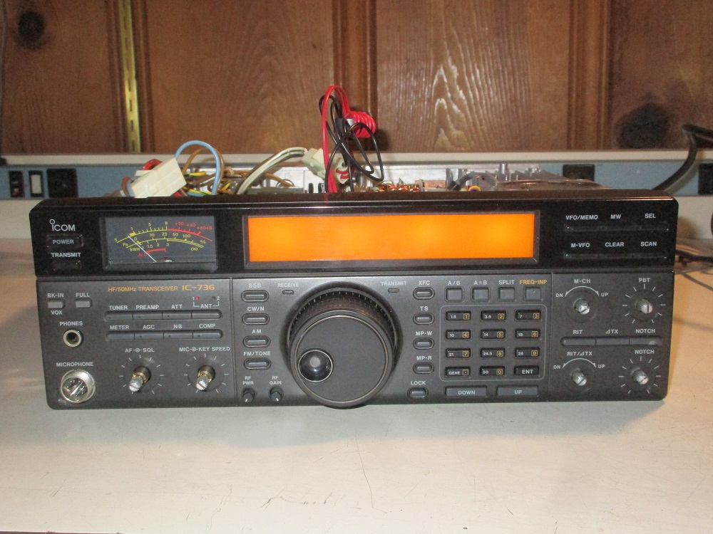
Under the covers, it was obvious, others have worked on it before. A metal shield that goes over the switching power supply is missing. The internal power connector to the front panel on/off switch had been disconnected. Connecting it up, it was verified that the switching power supply was working fine. About 29 VDC for the finals and 13.8 VDC to the rest of the rig. One front panel LED for ANT1 came on but the LCD backlight and the meter light did not come on. The meter light was found missing. A connector to the power transistor ( 2SB1015) which supplied power to to the LCD backlight was found to have been reversed.

Correcting the connection to that transistor brought the LCD backlight on but no display. There are a number of other regulators that create -5 VDC, +5 VDC, +8 VDC. In some cases there is more than one regulator for a voltage like the +5 VDC. So far it looks like all those regulators are working.
None of the front panel buttons other than the power switch work at this time. The assembly with the two potentiometers just to the right of the microphone connector was found to be loose as were two ribbon cables from the logic board under the front panel. The logic board has the LCD display drivers and the CPU so that may be the focus of attention at the moment.
The LCD pins were checked with an oscilloscope. No drive voltages were present. The inputs to the Sanyo LC8752A LCD driver IC was tested. The inputs in the magenta box were all low so there is no drive.
A TinySA Ultra spectrum analyzer with an antenna was placed next the the 30 MHz crystal ( in the red box ) for the CPU, X1, but nothing was found. It looks like the CPU has no crystal clock.

+5 VDC for the CPU comes in via connector J11. It was found to be present.
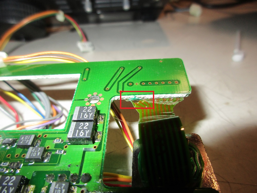
After taking photos of where all the cables go, the front panel assembly was removed. To get the Logic board out takes removing eight screws circled in red and un-soldering the front panel meter connections shown in the two yellow boxes. One of the screws on the far left is under the on/off switch.

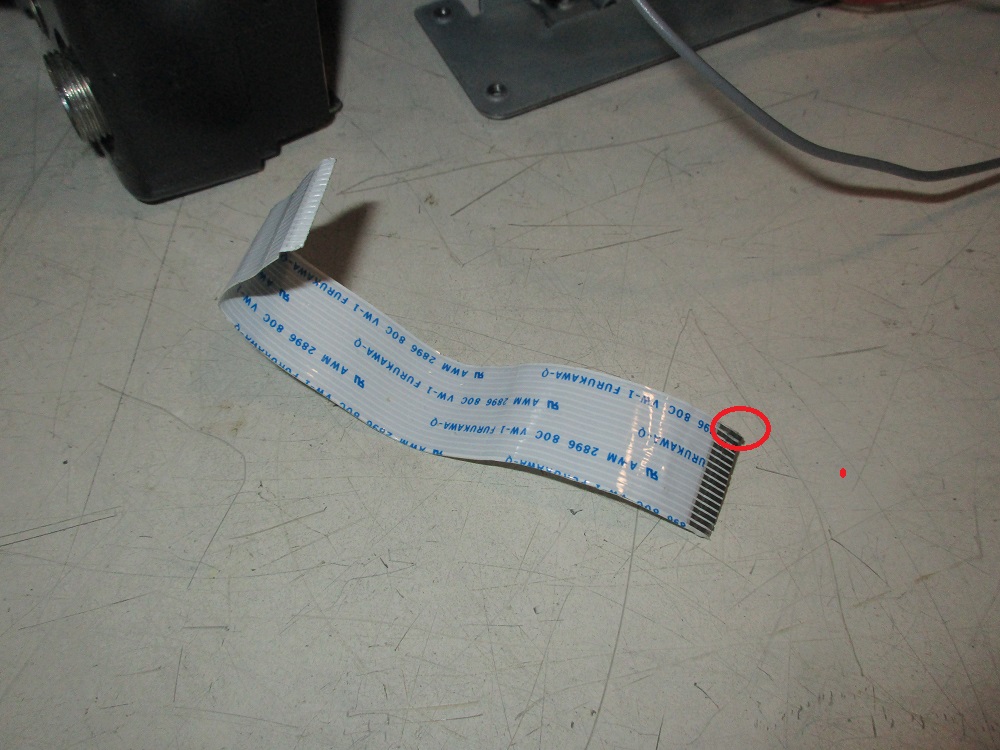
It was found that the flex cable from the Logic board to the microphone connector has been torn. Two traces are broken.
The front side of the Logic board shows the CPU. It was found that a repair had already been done to the CPU reset circuit. A leaded diode was used to replace a surface mount diode, DA114.
Removing the front bezel requires taking the tuning knob off. Under the rubber grip of the knob is an access hole to a set screw. Once the screws on the top and bottom of the bezel were removed, one more screw hidden by the tuning knob had to be removed.

After removing the bezel, the two potentiometers on the lower left of the metal front panel frame that had been loose could be tightened.
This is why the 736 is required to service the tuner in the PW-1. As can be seen the tuner control lines of the 736 are connected to the PW-1 main control board. Whatever digital information is being shared between the two units is not described by Icom. Icom also does not indicate that the firmware of any other Icom other than the 738 which is the same as the 736 minus the internal power supply is capable of this task, whatever the task it is.

These are the instructions after the two are connected together as shown above. There is no explanation of what is happening.

An HP6205C power supply was used to supply 13.8 VDC to the Logic board. The Logic board has a regulator which reduces the 13.8 VDC to 5 VDC which supplies the HD64180RP6X CPU and its reset circuit. The “6” specifies the maximum clock frequency of 6 MHz. All the proper voltages were found to the CPU but still no clock signal.
The clock crystal, Icom p/n CR276, was removed and tested as shown below.
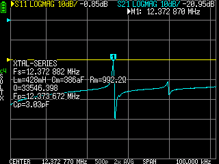
The resonance is at about 12.4 MHz and very lossy. No resonance could be found at or below the maximum clock frequency for the CPU. I happen to have a same size crystal at 5 MHz which tested as shown below.

The CR276 crystal was replaced with the 5 MHz crystal. The test of the Logic board was repeated but now there is a nice clock output at 5 MHz.
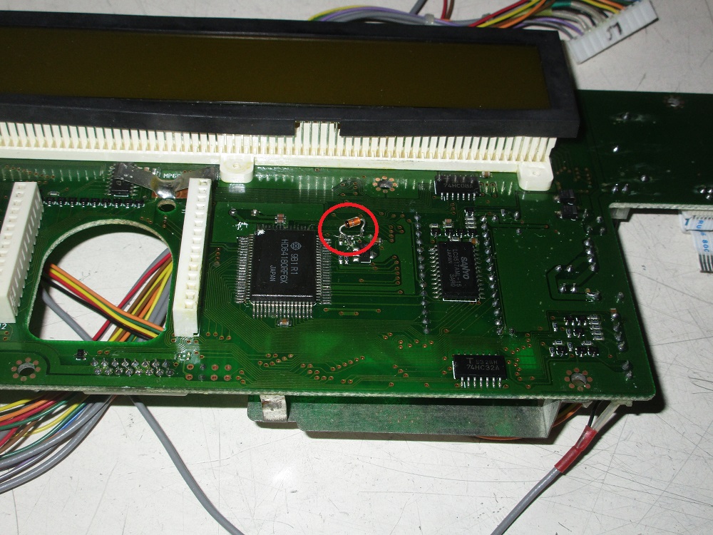
Below is a photo of the X1 crystal for the CPU. The letters and numbers shown in the photo are the only markings on the part. If anyone knows what the frequency of this crystal is please let me know.

Reassembly was started after the crystal was replaced but still no display or keyboard function. At the moment I am finding strange wiring that is hard to explain. The photo below shows P1. Notice that the schematic shows the coax going to pin 1 with the black ground lead going to pin 2, but as can be seen the actual P1 has it reversed. It was confirmed that pin 2 off the receptacle on the Main board is ground.
P2 on the schematic was wired that way too with the coax and ground reversed. Now I am going through all the connectors to see how many more are like this.

Today it was found in the block diagram of section 11 of the service manual, that the crystal for the CPU is 12.288 MHz which is not too far off from the 12.37 MHz measured by the nanoVNA except the loss of the crystal is so high that the oscillator will not oscillate.
The Logic board was removed and powered from an HP6205C power supply as before. All the used address lines from the CPU and the eight data lines were tested and were active. The only lines that were never active were CKS and TXS which are part of the clocked serial I/O port which goes to the LCD drivers. These are set up in firmware so either the hardware has failed or the firmware is corrupted or possibly some connection which I am not yet aware of enables the port.
With the bad crystal, the torn microphone ribbon cable, the CPU not driving the LCD drivers for whatever reason, the D6 replacement, I was fortunate to find a person selling a working Logic board for a very reasonable price. It should be here in a week or two, then perhaps some of these issues can be put to rest.
I did find this thread https://www.eevblog.com/forum/rf-microwave/icom-ic-736-front-panel-problem/
which describes the solution to a similar problem.
The replacement Logic board came in this Tuesday. Instead of using it directly, I decided to see if I could use it to troubleshoot the old board.
1. Both boards were powered up with an HP6205C power supply. The new board is working as described.
2. The shield covers were removed from both Eprom’s so the Eproms could be swapped. Swapping the Eprom’s had no effect which cleared the firmware from being the issue.
3. The 12.228 MHz crystal from the good board was swapped with the 5 MHz crystal in the old board. The good board worked fine with the 5 MHz crystal but the bad board did not work any better with the correct crystal.
4. Every input pin on each CPU was tested to see if the CPU was receiving any different inputs between the boards. No differences could be found.
5.This left the CPU. I have never seen any CPU chip fail so that left one possibility, a bad solder connection to the CPU
Solder wick copper braid that had been previously used to remove solder was used to reheat the solder connections of multiple CPU pins at a time. This works well compared to using the tip of a soldering iron because multiple pins can be reheated without creating solder bridges.
The pins in red were reheated first. Once that was done, the Logic board was powered on. The display immediately came on as shown below. The CPU problem was really just a poor solder connection.

The Logic board was reassembled to the front Switch board on the front panel. All the buttons now work but the main tuning knob RPG ( rotary pulse generator ) might have an issue. One of the three wires to it was broken but even after that was repaired the frequency decrements by itself although I can adjust the step size of the decrement using the “TS” button.
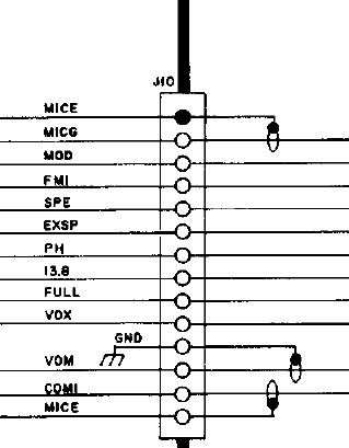
Earlier it was found that some of the coax cables appeared to have the shield and center conductor reversed at their connectors. Now that I have two Logic boards, it seems that the mistake was made at the factory. Below is a photo of connector J10 on the Logic board which has three coax cables connected at pins 1 and 2, 11 and 12, and 13 and 14.
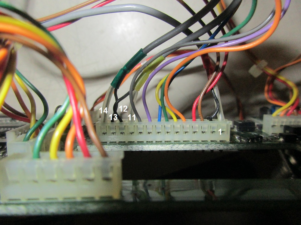
Here is the reverse side of J10. Notice that the center conductor of the coax connected to J10 pin 11 is grounded.

This is what the schematic shows. The coax at pins 1 and 2 has the center conductor connected to pin 2, the coax at pins 11 and 12 has the center conductor connected to pin 12, and the coax at pins 13 and 14 has the center conductor connected to pin 13. Every coax to the connector is reversed on the Logic board from the schematic.
Another problem has been these ribbon cables. Some of the metal tabs like the circled one are beginning to separate from the base material. When plugging in, the tab scrunches up failing to make contact. Some epoxy was used to try to improve this situation.
Coax Wiring Errors
I am a bit disappointed to find this situation in an Icom product, but with two Logic boards with the same errors, it likely is the case with most 736’s
I went though all the coax cables that originate from the front panel assembly to the main board. There are six. Three come from the Logic board J10, one from the Logic board J15, two from the AF Unit board J1. Every one of these coax cables is installed backwards from what the schematic shows with the connections of the shield and center conductor reversed. This seems to be a manufacturing error because these connections are solder in connections. It results in, for example, J15 of the Logic board having the coax center conductor grounded to the Logic board while the shield carries the signal.
The connections of these coax cables which all go to the Main board have to be reversed at the Main board as well. What I thought earlier was a former owner reversing the coax connections at the Main board from the schematic was in fact done at the factory.
Microphone
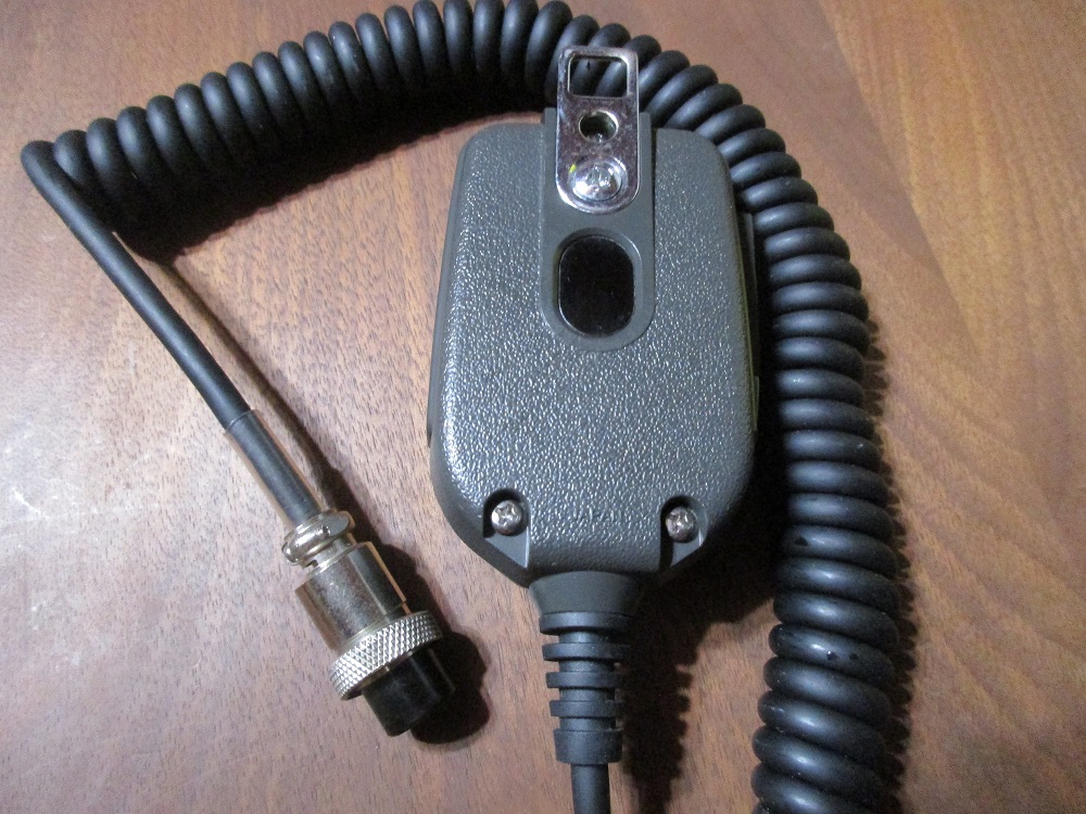
It took some time to find a real OEM HM-36 microphone. Most being sold are copies with the HM-36 label but no Icom name. A few have the Icom name but are made in China. Some of those vendors claim their product is the OEM product now made in China which is possible. It took some time but I was able to find a made in Japan HM-36 which is most likely OEM.

Logic Board
There was a set back with the Logic board however. In trying to determine if one the two RPG’s ( rotary pulse generators ) for the main dial or RIT was causing the decrementing frequency, the inputs from those parts to IC6, a TMP82C265BF peripheral interface, was tested. No changing inputs from either part was found. What was discovered what that the IC6 has been replaced but the job was not great. As shown below, there are missing pads on the pcb marked in red from that replacement. Also, two jumpers were found.
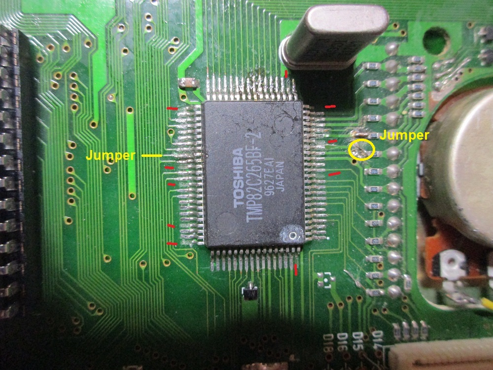
Compare that to the new Logic board.

Logic Board
After resoldering IC6, the signal on every pin was compared to the good Logic board. It was found the pin 55, PB06, was active on the bad board but at a logic low on the new board. PB06 is an input which tells IC6 that the CI-V bus is active. The bus was checked and it was indeed active. Resetting the CPU did result in the default state shown in the manual but the CI-V bus became active again shortly after. I ordered a USB to CI-V bus cable to connect to the computer. Perhaps then it can be determined why CI-V is active and what it is trying to do.
DXLAB Commander
I succeeded in installing Commander in the Lenovo laptop running Windows 11 by using the DXL Launcher. Commander should be able to control the 736 via CI-V.
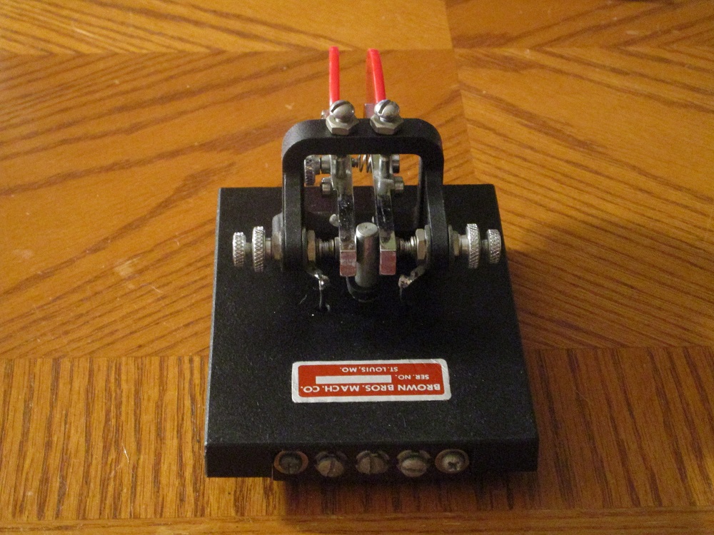
These are some notes about the Vibroplex Square Racer. It has been said that the Square Racer resembles a magnetic return version of Vibroplex’s other offering, the Bencher BY-1. They do share certain similarities.
Bencher of Antioch, IL was sold to Vibroplex in 2015 with the retirement of the principals. The Bencher BY-1 and BY-2 came out in 1974. The origin of the Square Racer seems to go back to Hamco located in Eureka, CA. The first model called the Scotia came out about 1978. Hamco was acquired by Vibroplex in 1982. Both designs apparently share lineage with the single paddle FYO design from the 1960’s. Of these designs, only the Hamco’s used magnets for the return.
Both the Bencher and Square Racer also allow setting different tensions for each paddle. The Square Racer does this with a separate magnet for each arm. The Bencher uses a single spring with a screw for each arm which can change the torque applied to the arm. The Square Racer feels like it can be set for a greater range of tension between arms mostly because the magnets can be set to a lower tension. In other words, the Square Racer feels like it can be set for lighter touch than the Bencher.
As with the BY-1, the Square Racer has two sheet metal arms bent in an L shape. Two screws shown below, allow the spacing of the paddles to be adjusted. I found these screws are not very tight but the vertical block they screw into is about 3/8″ thick so they might not move much. They affect the contact spacing as well as the paddle spacing.

An unusual feature of the Square Racer is that to set pressure on the fixed contact screws to keep them from moving, the contact assembly must be removed via the two screws shown below.

Once the contact assembly is removed, there is a nylon hex head setscrew that can be tightened against the screw carrying the contact to keep it from moving. I suspect the intent is to set some pressure against the contact screw prior to moving the contact screw into its final position. This is different from the BY-1 contact assembly which has a setscrew that is set against the contact screw at 90 degrees to the contact screw.

Shown below is the spring and plastic ball that holds the magnet assembly in place. On the right side in the photo, the ball and spring are still in position and sits flush with the bottom of the vertical block.
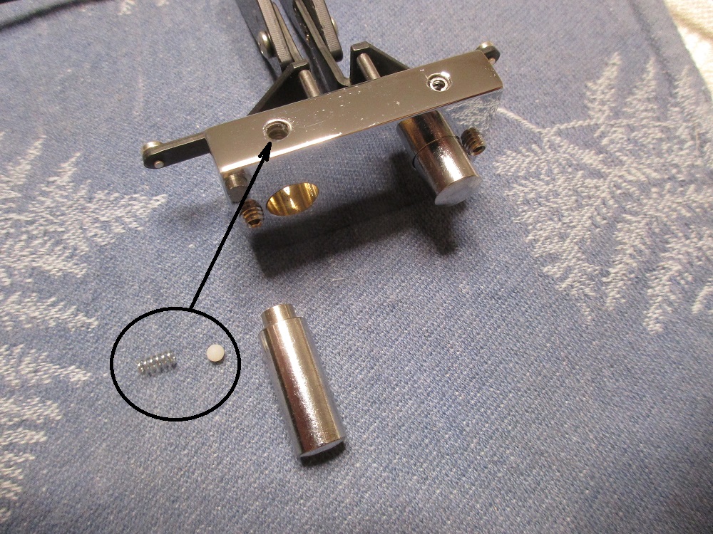
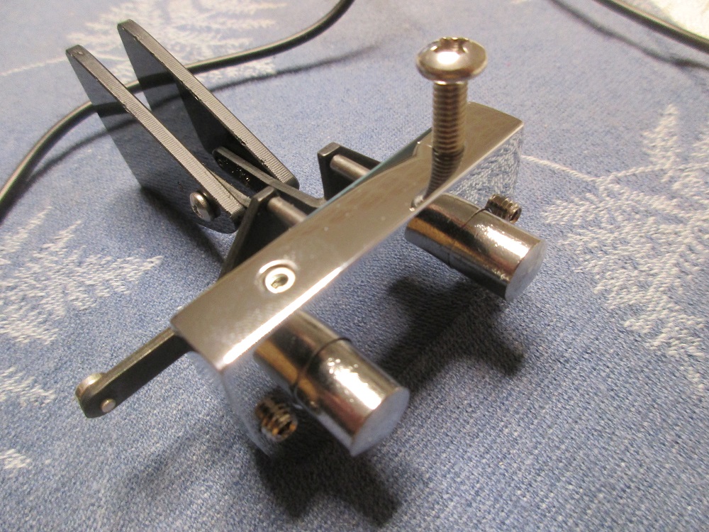
What presses the spring and ball against the magnet assembly is the screw that holds the vertical block to the base as shown below. Unfortunately, this system has a drawback. Depending the tolerance between the hole and the magnet assembly, the strength of the magnet, the strength of the spring, the pressure of the mounting screw in pushing the spring in, these factors all affect how close the magnet can be to the arm before the magnet can overcome the retention forces and slip forward to attach itself to the arm. It was found on the left side, the magnet would slip forward once it is within about one millimeter of the arm but on the right side the magnet can be closer.
This makes it difficult to set and hold higher tensions which is the reverse of the BY-1 where higher tensions are easily set.
Below is a photo from this web site.
https://www.qsl.net/n0uf/hamco.htm
It shows the original “Scotia” paddle by Hamco upon which the Square Racer is based used set screws from the top to hold the magnets and contact screws in place.

From the same site is this photo of the “Carson” also made by Hamco. As can be seen, the top set screws to hold the contact screws are gone although the magnets are still held in place by set screws.

Recently my Bencher BY-1 was traded for a Bencher ST-1 which is the single paddle, non-iambic version. Although these two paddles bear a strong resemblance, they are more different than one might expect.

The ST-1 is much simpler and has fewer adjustments.

These are two popular paddles that are mechanically much different. This is a comparison of the mechanisms and their unique characteristics
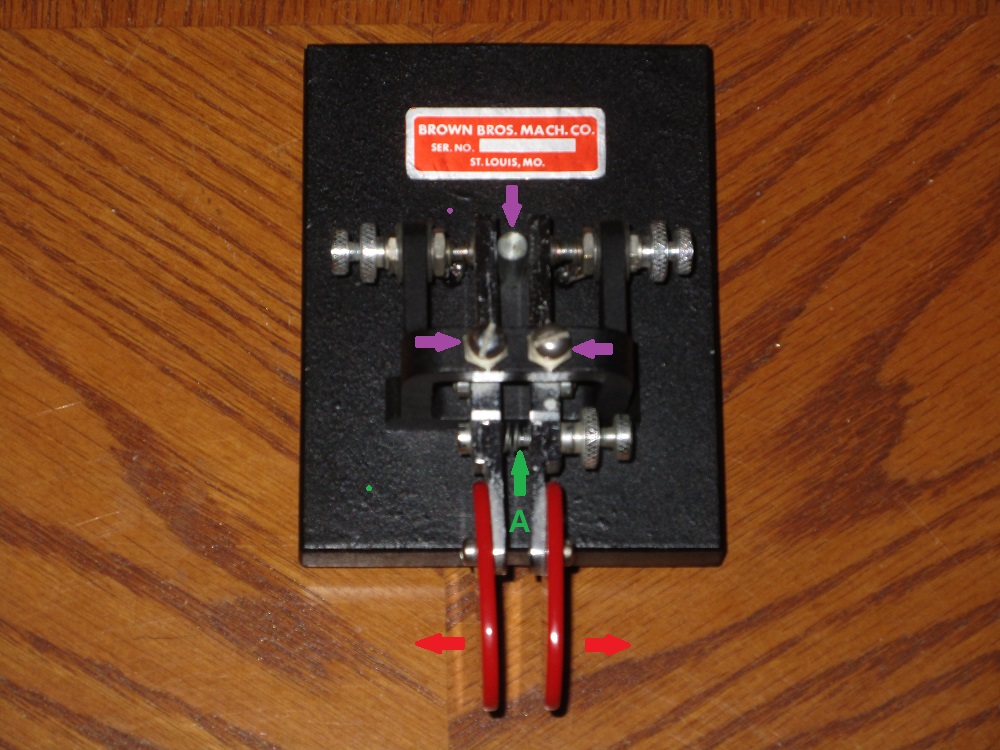
The Brown Bros original BTL ( not the later BTL-A ) uses trunnions or axles in each paddle lever assembly which are held in place via pivots in the base and the arch with adjustment screws to hold the lever assemblies and remove play.
These are the base pivots.

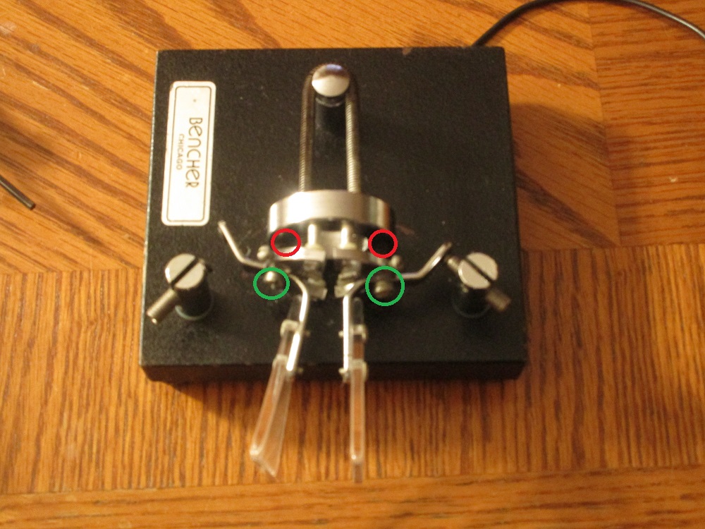
The BY-1 has no adjustments to remove play. The Bencher design uses the lever assembly return spring to pull each lever assembly onto two pivots. This eliminates adjustments but is also responsible for the “fly apart” problem associated with this design. Since the return spring is the only force holding the lever assemblies to the base, those with heavier fists have been known to be able to knock the lever assembly off its pivots. In the photo below, I lifted the left paddle assembly off its pivots so the pivots can be seen.

Newer BY-1’s have two additional screws, one for each lever assembly that prevent pulling those assemblies off like I did above.

The BTL has no real adjustment for the spacing between the paddles other than mounting the plastic paddles inside, outside, or one inside and one outside the metal lever arms. The spacing is governed by the positions of the trunnion pivots and the round stop at the back. The BY-1 has a two screws that continuously adjust the position of either lever arm independently. The red circles in the photo below show where the black Torx T-8 screws protrude and push against the rear of the screws circled in green to adjust the position of the paddle.
The BTL levers have a return spring between the lever assemblies just back of the paddles shown at A in the photo below. A screw adjustment allows more of less compression of the return spring which pushes the levers apart to their rest position. The trunnion positions and the round stop with the purple arrows fix the rest position of both paddles.
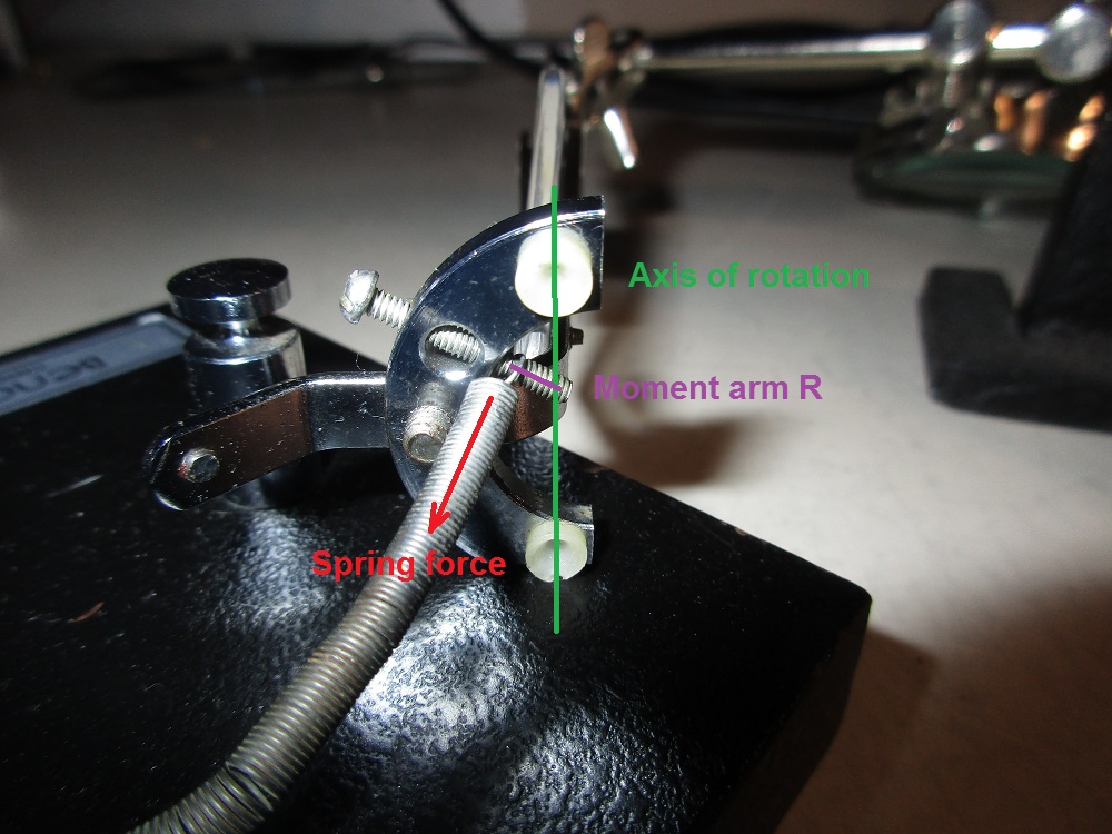
The BY-1 return mechanism works via torque with torque being defined as T = moment arm x force. In the photo below, a lever assembly is removed to show the two pivots about which the lever assembly rotates. It also shows the spring exerting a force against an adjustment screw. The spring is positioned by the screw so that it’s position coincides with a point on the axis of rotation. Under this condition, the moment arm = 0 so the spring exerts no torque to rotate the lever assembly to its rest position.

The photo below shows the adjustment screw has moved the spring away from the axis of rotation, creating the moment arm R. Torque = R * spring force so there is now a torque to rotate the lever assembly to its rest position. Since each lever assembly has its own adjustment screw, the torque to return each assembly to its rest position can be different.
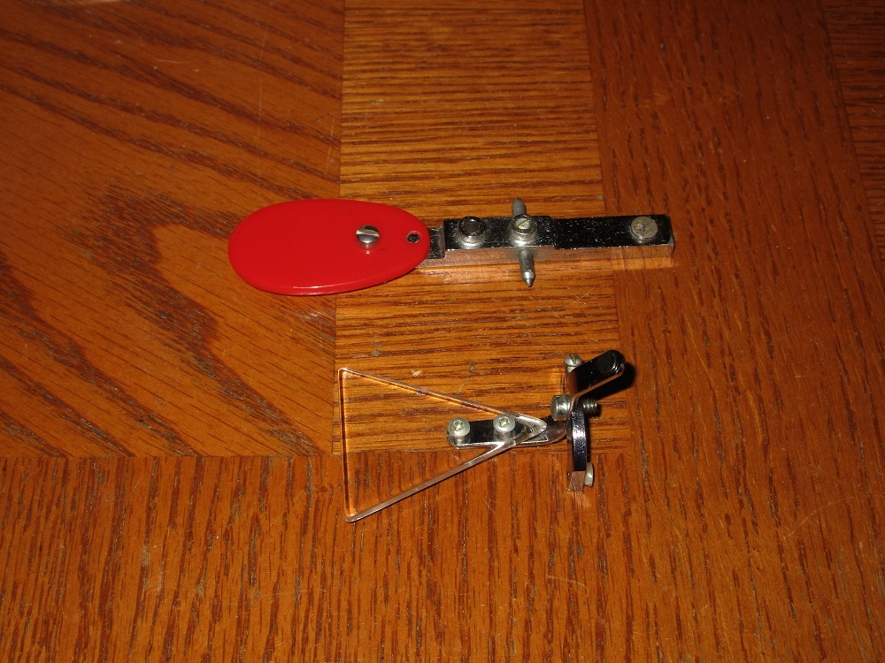
The BTL makes a sharp clicking sound when operated. The BY-1 makes a much duller, muted sound by comparison. I suspect the reason for this is that the BTL lever looks to be bar stock where the BY-1 lever is folded sheet metal. Below is a photo of the lever assemblies of the BTL and BY-1. The weight of the BTL assembly is 0.9 oz., the BY-1 assembly weighs in at 0.4 oz.
From kinetic energy = ( mass ) x ( velocity ) **2, the heavier object will require more energy to move. The return spring also needs to exert more energy to return it to the rest position in the same amount of time.
The heavier stiffer BTL lever makes contact with more kinetic energy and less flexing. The BY-1 lever assembly is much lighter so it makes contact with less energy and some of that energy is absorbed in flexing. It did not take much effort squeezing the levers together to distort the sheet metal levers. This also explains some review comments about the BY-1 having a spongy feel.
There are a few other physical differences that can be seen below. The BTL paddles are higher even though the base looks lower. Also, the BTL weighs in at 2 lbs 2.6 oz, the smaller looking BY-1 weighs in at 2 lbs 14.1 oz.

There are paddles that bear a strong resemblance to the BTL and BY-1.
This is a Vibroplex paddle that resembles the BTL.

The MFJ 564 resembles the BY-1.

I acquired an old 1993 Whitfield Advantage II-T fireplace insert on Saturday, January 20, 2024. Downloaded the manual an managed to get it installed on Wednesday, January 24th.
I have worked on more modern pellet stoves like the ones sold by Lowe’s but this old timer was an interesting study.
First it was not clear what the air paths were, how air wash worked, and how to handle the fact that this insert model had no ignitor or damper like the non-insert version.
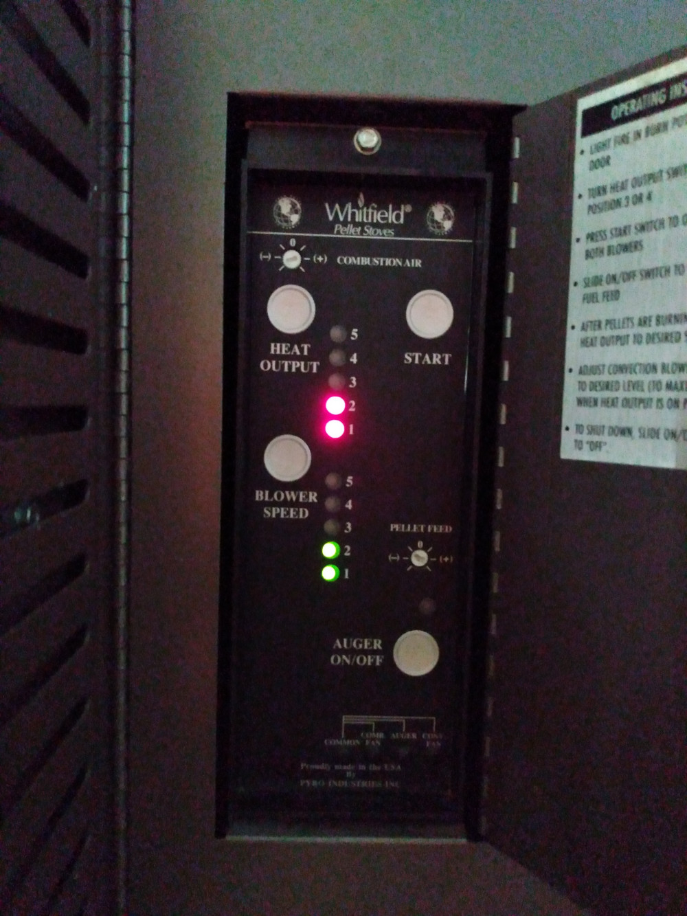
Controller
Air Flow
Most of the air for combustion comes in through the smaller diameter pipe at the back of the unit. This air almost immediately exits into the back of the cabinet.
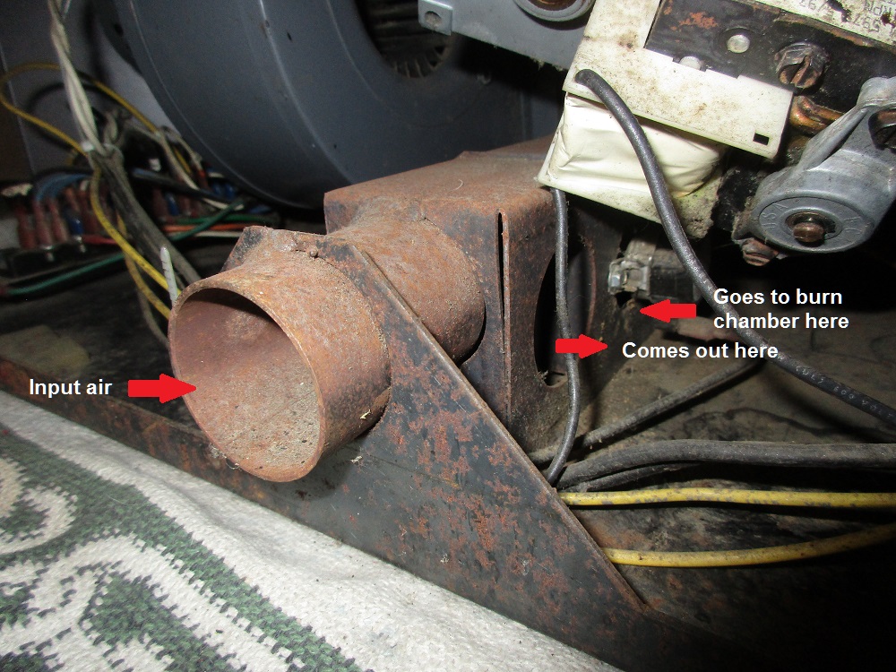
Air inside the back of the cabinet is pulled past the sensor show below.
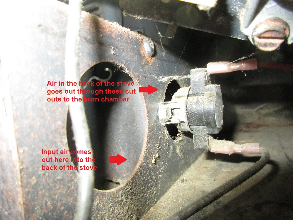
That air comes out under the grate which holds the pellets as they burn. The grate is removed to show where the air from the back comes out. The green rectangle represents where the combustion blower input is located. It pulls the air up from under the grate and then through the two openings on the sides shown by the two vertical red arrows. That air then enters the combustion blower at the green rectangle and is expelled by the blower through the larger 3′ pipe on the back of the unit.

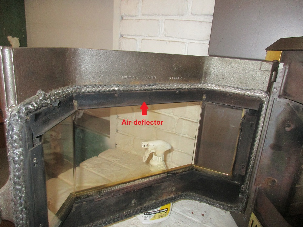
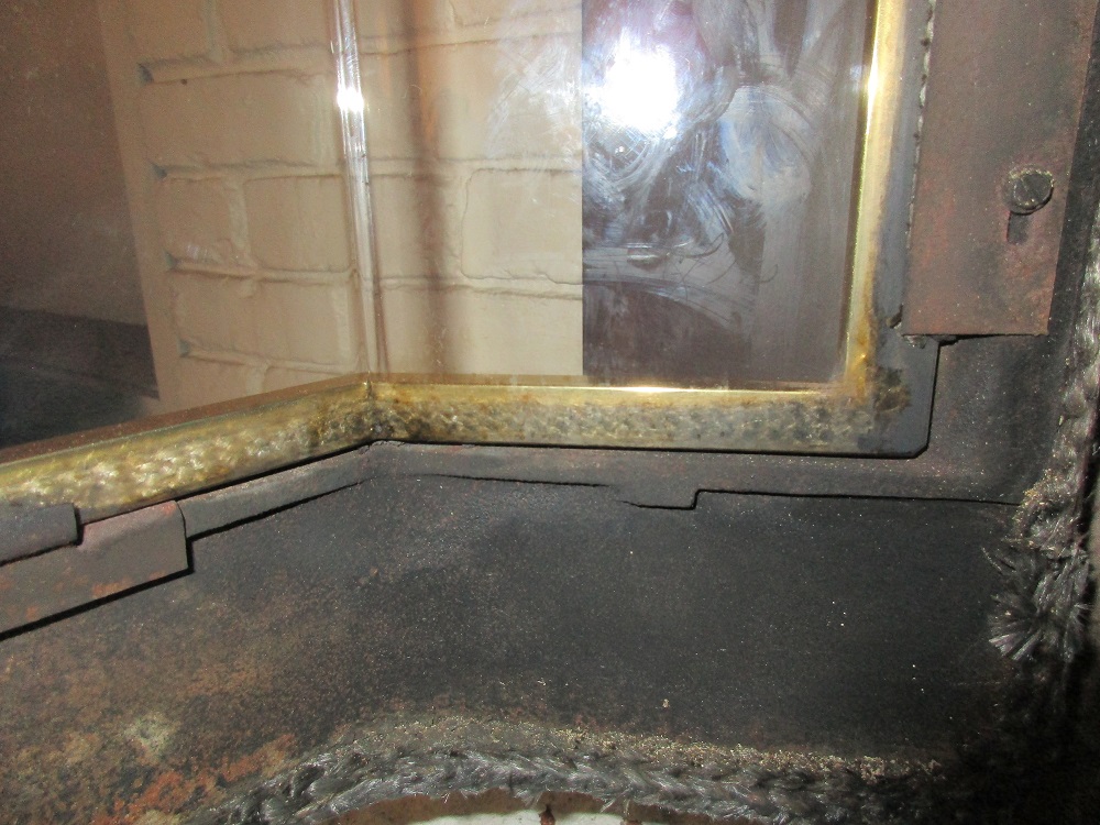
Air Wash
The above is the primary supply path for air to the combustion chamber but not the only one. The air wash system is another source of combustion air. Below is a metal strip at the top of the window that acts as an air deflector.
If the metal strip is removed, it can be seen that the window is not sealed across the top.
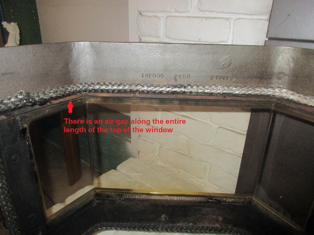
A close up of the gap.
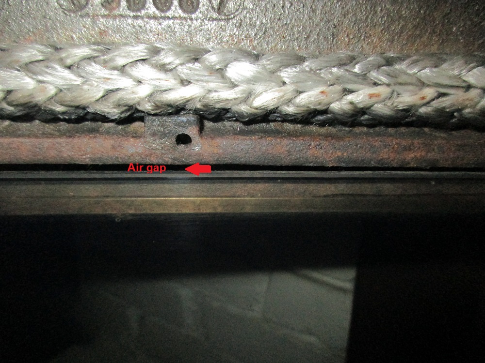
An old envelope is inserted between the brass trim in front and through the gap for cleaning.

On the other three sides of the window, rope is used between the brass trim and window to prevent air flow.
Auger Timing
To test the auger timing, a digital storage oscilloscope was used the measure the auger on/off times depending upon the position of the trim control and the Heat position selected. The “min” position of the trim control is counter clockwise, the “max” is fully clockwise, the “mid” position is in between.
Heat Position On Time min On Time mid On Time max Off Time min Off Time mid Off Time max
1 0.8 1.52 2.12 8 7 6
2 0.8 1.52 2.12 5.36 4.88 4.4
3 0.8 1.48 2.08 3.0 2.96 2.8
4 0.8 1.44 2.2 2.24 1.96 1.72
5 0.84 1.52 2.12 1.72 1.44 1.12
Pellet Drop Rate
Pellet drop rate was measured by collected samples into a glass jar in one minute intervals. Multiplying the average weight of the collected samples by 60 to reach an hour then dividing by 16 for pounds/hour shown below. The “Min”, “Mid”, and “Max” refer to the position of the auger trim setting with “Min” being counter clockwise.
Heat Position Min Mid Max ( lbs/hr )
1 0.45 1.05 1.35
2 0.56 1.56 2.06
3 1.24 1.99 2.55
4 1.73 2.63 3.38
5 1.83 3.00 4.46
Thoughts
These older style stoves are mechanically more complex resulting in more nooks and crannies for ash to hide out.
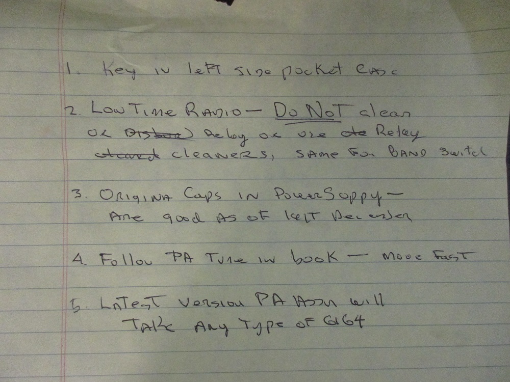
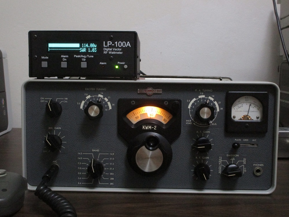
Purchased on Saturday, November 4, 2023 for $650 from Wendell Peterson ( K6POU ) with items shown.
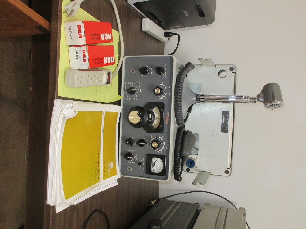
Including the PM-2 power supply, the manual, an Astatic C-10 microphone, an Electro-Voice 600E microphone, two spare 6146B’s, and an outlet strip to use as an on/off switch.
The seller, a retired physicist with Lawrence Berkeley Labs, left this note. He said the KWM-2 is from 1964; that the first owner kept it for 21 years, that he bought it in 1996 so has had it for about 27 years. He seemed genuinely concerned about selling to someone who would know how to care for it.
This is a photo of the neutralization capacitor which looks to be an air variable.
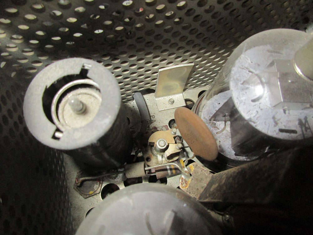
These are two of the three relays, but they are open frame and not the later sealed units. The one not in the photos is the VOX relay.
I noticed that the relay towards the rear has contacts that do not have very much contact material but under a magnifying glass do not show much wear. These relays are under a metal cover but it did not appear that the cover had ever been removed before.
The serial number,

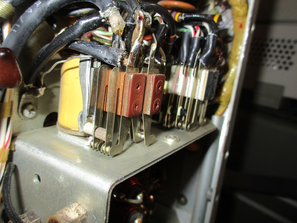
The power supply 100 ufd, 350 WVDC capacitors do not look well. The seller related to me a story about how he had the unit sold for the asking price last December but during the demo, he thought the buyer had damaged the finals by taking too much time to tune it, then backed out of the deal. Not sure that is the case, since the seller was not aware of the condition of these capacitors.

All the 100 ufd, 350 WVDC capacitors were pulled. They all look to have been leaking to some degree.
After they were replaced, The PM-2 was reattached to the KWM-2. The fuse blew when the KWM-2 was turned on. I found that the KWM-2 has a rather specific turn-on sequence. Once I followed the sequence, the fuse did not blow. I was told that the finals were damaged by a prior buyer attempting to tune up, but since nothing out of the ordinary occurred during the turn-on sequence, I went ahead with normal tune-up on 20 M.
It looks like the problem was just the bad HV capacitors in the power supply. Tune-up was successful on 20 M with nothing out of the ordinary occurring.
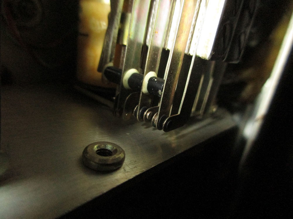
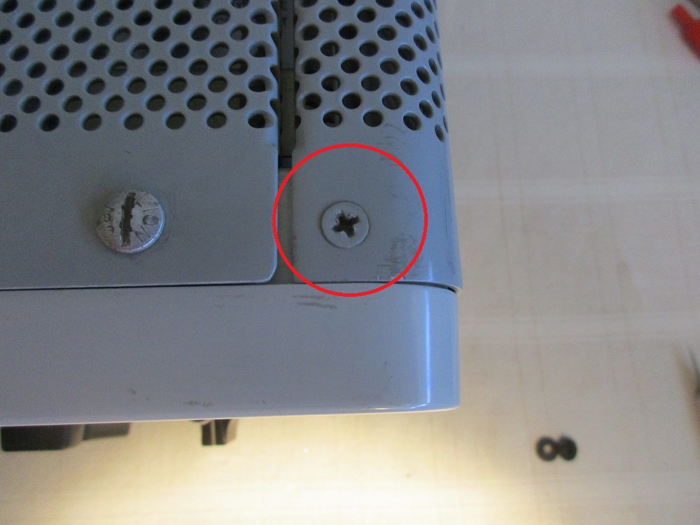
The most challenging mechanical issue was the two screws that are in the upper, left and right corners like the one shown below that holds the case to the chassis. Underneath the screw is a large flat washer, a split ring lockwasher, and a nut but there is no room to hold these parts in place while the screw is attached. I had to resort to using a glue stick to glue the nut, lock, and flat washer to a stiff piece of cardboard which was used to hold all the parts in place under the screw position so the screw could be inserted through all of those parts.
I looked into relays K2 and K4 both sealed and open frame. The sealed relay K2 is Collins p/n 970-2439-010 which is Allied Control p/n T163X-96. Sealed relay K4 is Collins p/n 970-2439-020 which is Allied Control p/n T163X-97.
Surplus sales wants $149 for the above K2 and $165 for K4. I found both the K2, 4 relays on eBay for $64 each.
Open frame relay K2 is Collins p/n 970-1940-00 which is C.P. Clark p/n B106703. Open frame relay K4 is Collins p/n 970-1941-00 which is AEMCO p/n 110-3680. Surplussales does not have these but I found both on eBay for $16 each. These relays are all NOS. I ordered a K2 and K4 open freme relay for $32 plus shipping.
This article is from the Collins newsletter Pulse for August, 1973 page 14.
The two open frame relays for the KWM-2 ordered from eBay arrived today but the box contained one opened ( for photo ) and one still sealed package of the C.P. Clark relay p/n B106703. These relays appear to be government issue with government and the manufacturer’s p/n number but no Collins p/n. A message to the vendor has been sent that two of the same relay arrived with the AEMCO relay not being one of them unfortunately. The opened package is lined with aluminum foil.
The new microphone gain potentiometer with on/off switch, 6CL6, and both K2 and K4 relays arrived before Thanksgiving.
Output power is more than 100 watts on all bands at 230 mA plate current with the new mic gain control and 6CL6 driver but an anomaly showed up. Metering the grid current showed considerable drift although output power and plate current showed no change.
These are the results of measuring the 10% tolerance carbon composition resistors for drift.
Ref Value (ohms) Measured Value
R1 47k 46.9k
R2 1Meg 1.093Meg
R3 180 197
R5 470k 490k
R6 1k 1.073k
R7 47k 46.3k
R40 100k 102.7k
R44 270k 279.4k
R49 100k 102.1k
R50 47k 50.1k
R51 390k 371.7k
R52 390k 352.7k
R54 1Meg 1.10Meg ( at 10% )
R55 220k 239.7k
R87 6.8k 9.57k ( out of spec )
R88 820 909 ( out of spec )
R135 1k 1.084k
Out of 17 parts measured, two are out of specification but there is uncertainty about whether these are original parts or replacement parts or if these parts had been subjected to undue stress from other nearby component failures.
R88 is the cathode resistor for the product detector, V15B, and R87 is the plate filter resistor for the same. The photo below shows in green components that were replaced near V15B. C106B which was replaced connects to R87. In red are the two out of specification resistors. R90 which is not out of specification connects to R87 but it’s lead length is too short. R90 is actually soldered to R87’s wire lead extending to the left which is soldered to a post.
This is the only area where so many parts had been replaced.
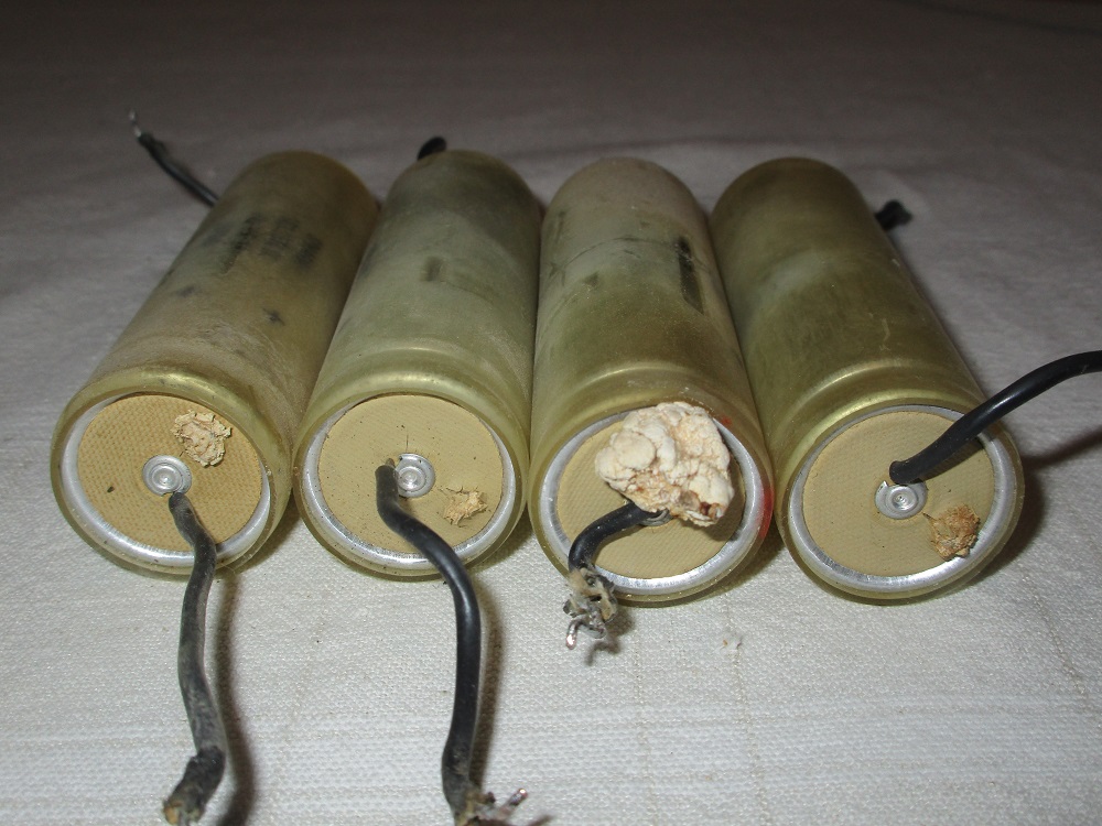
The seller said that he had taken C106 out and re-stuffed the can so it was a bit of a surprise to see added underneath as shown in the photo above. I removed C106A and B to get access to the original C106. Removed C106 and found that he had re-stuffed the can but with 22 ufd, 350 V capacitors. The can is marked 30 ufd, 350 V. The capacitor above to the right of the can is the 33 mfd, 350 V C106B I removed from underneath the chassis. It measures 1.3″ long. The can is about 2.5″ tall but the two bakelite parts at the base take up about 0.25″ leaving about 2.25″ for the two capacitors. The 22 ufd, 350 V parts are just under 1.1″ long so two of them fit.
Al electrolytic capacitors have better volumetric efficiency today. I have on order two 33 mfd, 400 V, 105 degree C. capacitors that are 16 x 20 mm, smaller than the 22 mfd, 350 V capacitors currently in the can.
My manual shows that C106 is a 30, 20, 15 mfd capacitor all at 350 V which differs from the 30, 30 mfd, 350 V part actually installed. There is a 33 mfd, 350 V part installed as C106c. The schematic shows it was where the 15 mfd section was used. The C106A 20 mfd section is shown as connected to the out of specification R87.
When this is sorted out, I will get back to the drifting grid current issue. My recollection is that upon initial tune up on 80 M, the grid current did not seem to drift. I did not see that until I tuned up on 10 M. After seeing plate current reading of 230 mA and 102 watt output on the LP-100A, the switch was changed to see what the grid current was doing. It appeared drift towards zero in about 5-10 seconds. There was no change in plate current or output power when it happened.
The Mallory 30/30 mfd/ 350/350 V capacitor in the prior photo is not an original part. Manuals from 1959 to 1978 for the KWM-2/2A show C106 is a 30/20/15 mfd/ 350/350/350 V capacitor. The 1978 manual identifies the manufacturer as Sprague with Sprague part number D29413. A Sprague 1967 catalog C-318 shows that electrolytic capacitors with the “D” prefix fall under heading of “special purpose capacitors”. The D29413 is not listed in the catalog however. The D29413 does show up as purchased by the government under p/n 5910-00-985-3870 identifying Sprague as the manufacturer with p/n D29413 giving it’s characteristic including it’s dimensions as 1″ in diameter by 2.563″ tall. These are the same dimensions as the Mallory part found in the KWM-2. For a proper restoration then would require re-stuffing of the Mallory with a 15, 20, and 30 mfd capacitor at 350 V and labeling it as such.
All the carbon composition resistors in the PM-2 power supply were tested. None where out of specification.
Ref Value (ohms) Measures Value
R1 100k 104.3k
R3 270k 290.7k
R4 270k 261.1k
R5 20 20.5 ( this resistor has been replaced with a metal film part )
R6 47 51.3
R7 3.9k 4.141k
R9 4.7k 5.03k
R10 270k 273.1k
R11 270k 283k
I now know why these Collins carbon composition resistors are so good. The information is in the 1978 manual where the mil-spec part number is given in addition to the Collins part number.
I picked the following resistor out of the 1978 online manual as an example. Mil-spec p/n RCR20G680KS which is Collins p/n 745-1303-000. These resistors conform to mil-spec Mil-R-390008C which includes a reliability specification.
The last letter on the end “S” indicates the highest reliability grade with a .001% failure rate / 1000 hours.
https://federalconnectors.com/files/specsheet/resistors/rcr.pdf
These resistors are still available but being mil-spec, they are $2.50 each.
https://federalconnectors.com/RCR20G680KS
This is the only instance I have run across where a manufacturer of a commercial product is using not just military grade parts but the most reliable military parts.
Some general comments first today.
I can see why the teflon wired versions of the KWM-2 may be more desirable. I found working on this one that there are no shortage of solder lugs or tie points which are so loaded with components and wires that it was necessary to use a heavier Weller soldering iron to remove or add back a component. It is especially bad if a prior owner cut the leads off a part leaving the remnant in the solder lug leaving no room to add a replacement part back properly. The heavier iron required a lot more care due to the crowded conditions. Places were found where a prior owner had not been quite so careful with wire insulation obviously damaged by heat from an iron.
The 28.4-2.6 MHz crystal arrived from Canada. The KWM-2 only has 14 crystal positions. The KWM-2A has two banks of 14 crystal positions. This allows adding the WARC bands painlessly. If WARC bands are important then the 2A is the desirable version.
The following work is to replace the out of specification resistors R87 and R88 in the product detector circuit. Also, to determine if the C106 capacitor found in the unit is the original part.
After reviewing manuals from 1959 to 1978, it is clear that the Mallory 30/30 mfd / 350/350 V can electrolytic part is not original. The service manuals for all years show that C106 is a 30/20/15 mfd/ 350/350/350 V part. C106 is made by Sprague with Sprague p/n D29413. The “D” designation is a for special part so it does not appear in a Sprague catalog. The special part does have assigned to it a NSN ( national stock number ) of 5910-00-985-3870. A search on the procurement number shows all the specifications including the size of 1″ dia by 2.56″ tall. Those are the same dimensions as the Mallory part.
I bought 33 mfd, 400V, 22 mfd, 400V, and 15mfd, 450 V parts to fit inside the Mallory can. These are 105 degree C parts vs the original 85 degree C part.

I make it point to clearly label what is currently in the can.

I set the bias for the 6146A finals to 50 mA up from 35 mA. The manual recommends 40 mA barefoot but if used with an amplifier, 50 mA. It would be interesting to see if there is a difference in the IMD between these settings.
I began to investigate the grid current drift. The schematic below from 1962 shows that back then, the “Lock” and “Tune” positions ground the ALC output so there is no ALC during tuneup.

Between, 1962 and 1978, the design was changed.

ALC is now active in “Lock” and “Tune” Emission modes. The 1978 manual on page 3-2 describes the components boxed in green this way, “The voltage is filtered by C159, C160, R118, and R119 ( which also determine the ALC time constants ) and is used to control the gain of V4A and V7.”
I ran a time and frequency domain analysis of this network including C158 to see its behavior. This is the time domain response to a step input. As can be seen it has a very slow response primarily determined by the values of R118 and C160 which create a cutoff at about 0.5 Hz. I suspect this is a good part of the reason for the slow drift in the grid current found.

This is the frequency domain response. The peak in the response is created by C159.
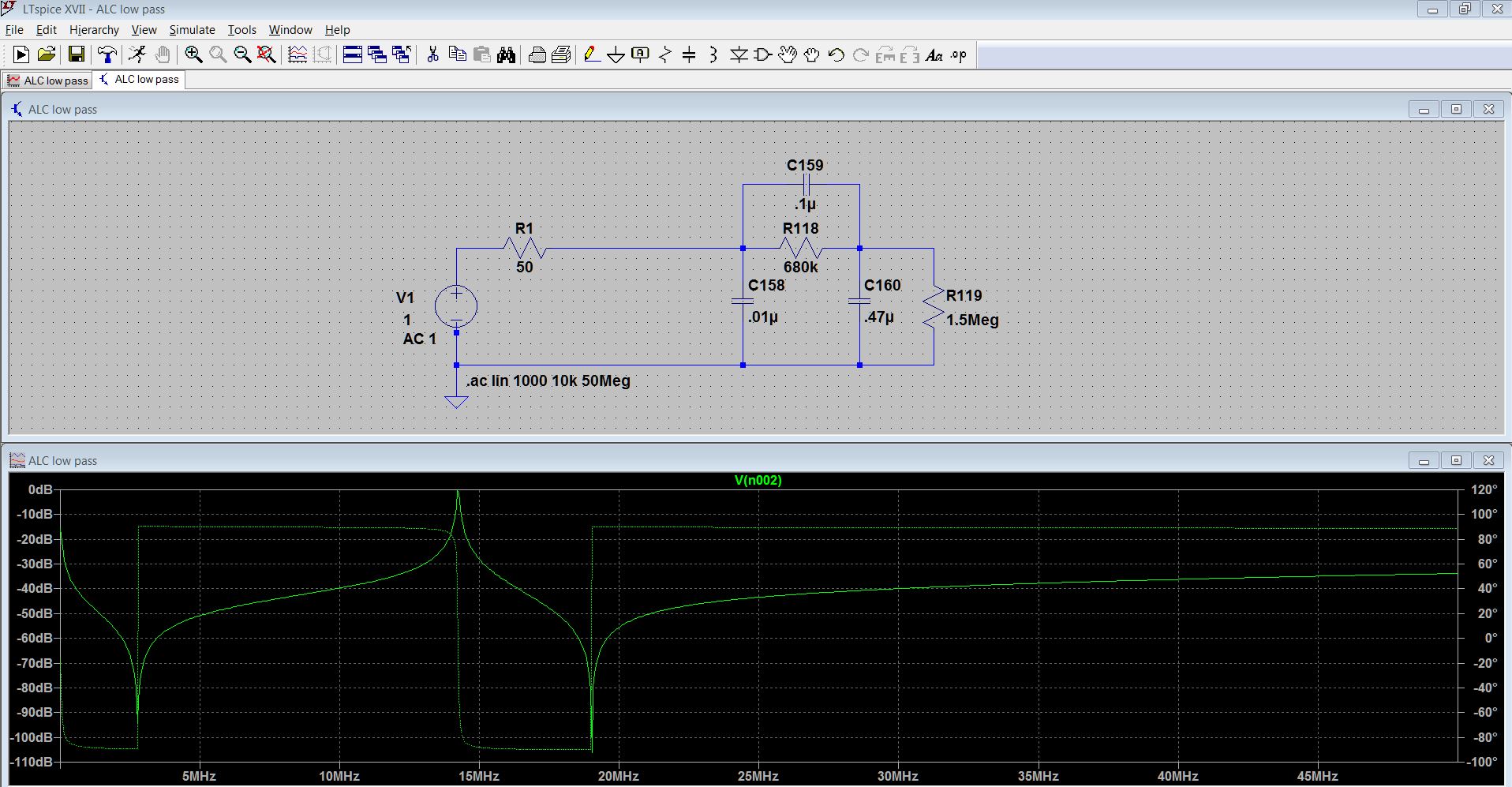
If C159 is removed, the response is without the peak. I am not sure why this was done but I suspect there is a good reason.

The reason for the change to allow ALC in “Lock” and “Tune” modes is on page 7-12 of the 1978 manual. It states “R11, 470 ohms, added and R190, 1500 ohms, was 2200 ohms. These changes shift the ALC line bias to reduce transmit gain variations between LSB, USB, and CW positions versus TUNE and LOCK positions of the EMISSION control. If repairing this circuit, recommend that the same configuration be maintained.” This unit has not been updated to the level of the 1978 schematic since R190 was found to still be 2200 ohms.
Below is a capture with the yellow trace monitoring the RF output. The blue trace is the voltage at C11 which feeds into the grid of V4 from the ALC detector.

Once “Lock” mode is on, there is 112 Vp at the RF output port into 50 ohms which is about 120 watts on 80 M. The V4 bias can be seen to shift down to -1.72 volts from -1.44 volts.

I also noticed that the tuneup procedure changed between the 1962 and 1978 manuals. The 1962 procedure results in a positive grid current reading which may be drifting in the “Lock” mode of the Emission switch. The 1978 tuneup procedure results in a zero or even slightly negative grid reading.
It looks like it would is advisable to obtain some Bristol drivers for working on the KWM-2. I was able to remove the main tuning knob with an Allen wrench but a close look at the setscrews show they have splines. The “zero set” knob is the same but smaller.

This is the KWM-2A parasitic suppressor.

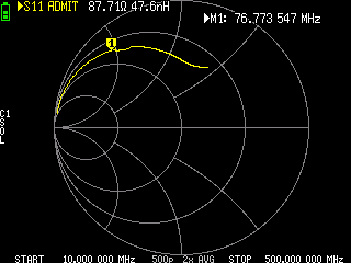
The S11 frequency response.
IMD preliminary tests
IMD with 100 watts peak power

50 watts peak power
25 watts peak power

Peak power was determined by using the LP-100A power meter to calibrate a scope volt reading for 100 watts with a CW signal. The two tones were then introduced as shown. The peak power was set to 100 watts using an HP6205C power supply supplying a negative voltage to the ALC input on the KWM-2.

Collins has a 30 dB IMD specification so this one is just squeaking by. These are preliminary results to see how things stand since the driver, final, and feedback neutralization have yet to be done. Tones used were 700 Hz and 1900 Hz. Spectrum analyzer used was TinySA Ultra. Oscilloscope used was the Rigol DS1102E.
Neutralization
The KWM-2’s have a relatively complicated neutralization method involving three variable capacitors shown below. The procedure is in the manual but to give an idea of what needs to be done. C184 for PA neutralization requires B+ be removed and a jumper between two rear panel connectors J5 an J6 removed. Removing the B+ with the 516F2 power supply only requires removing a tube. The PM2 power supply had to be opened up to disable the B+.
The driver neutralization requires adjusting C117 after removing power to the filament of the 6CL6 driver.
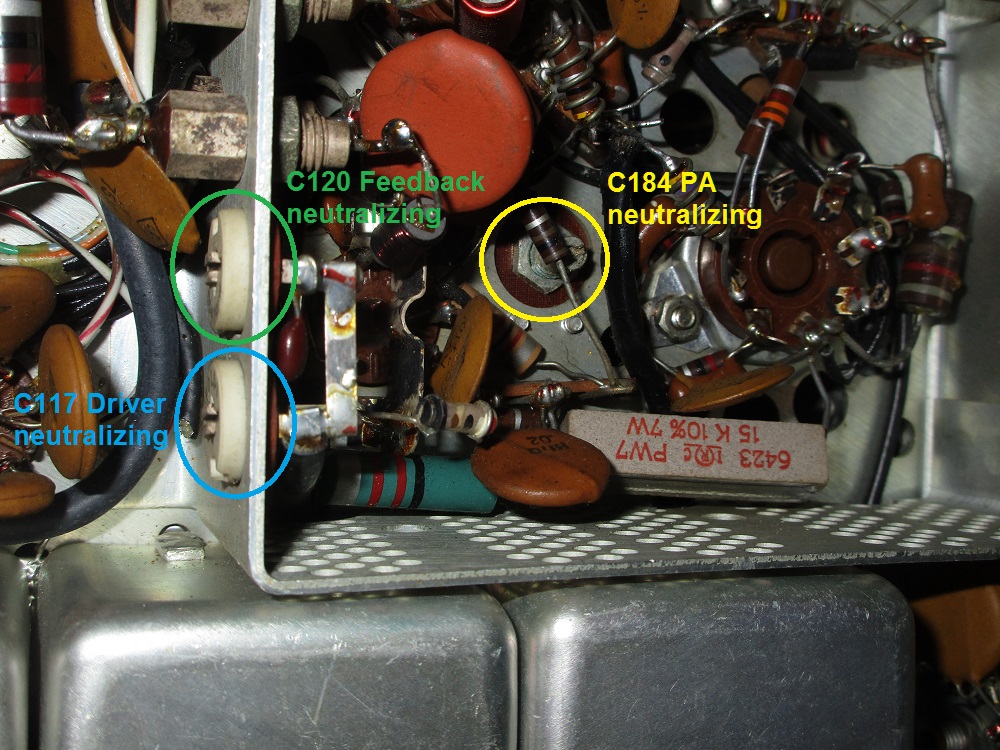
In both cases above, Collins uses a dummy load with an RF probe across it. C184 and C117 are used to minimize the signal at the dummy load. I departed from that by using high power attenuator connected to a scope. Then C184 and C117 were adjusted to minimize the scope signal.
The adjustment of C120 ensures that the plate dip and grid dip occur at the same setting of the PA tune control. It was found that all three capacitors were not set optimally for the tubes currently being used.
IMD Tests
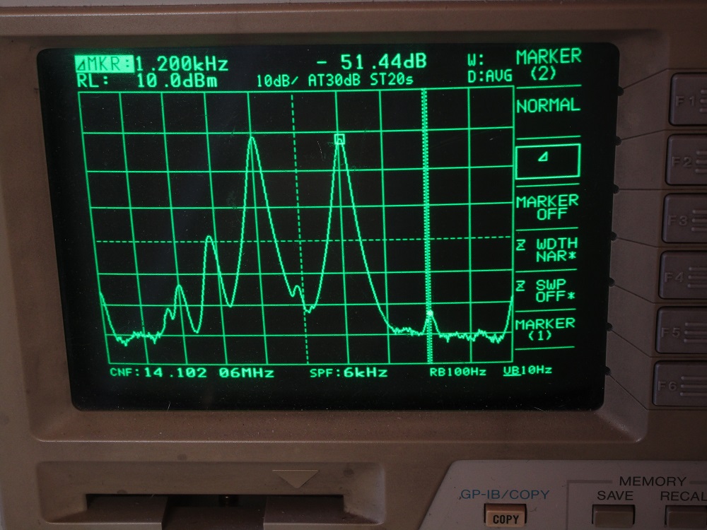
These IMD tests were done with two attenuators between the KWM-2A and a spectrum analyzer. The insertion loss of the two attenuators was measured with a nanoVNA at about the test frequency. Measured insertion loss was 45.32 dB so a 100 watt output from the KWM-2A would be about 4.68 dBm at the input to the spectrum analyzer.
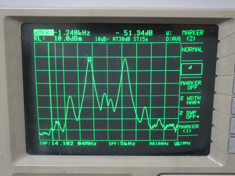
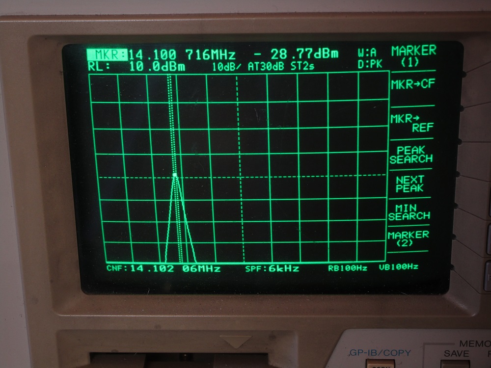
Here is a spectrum analyzer view of one 700 Hz tone introduced at the microphone input with the output power of the KWM-2A at about 100 watts. The plate current is just under 230 mA.

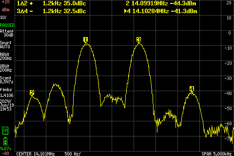
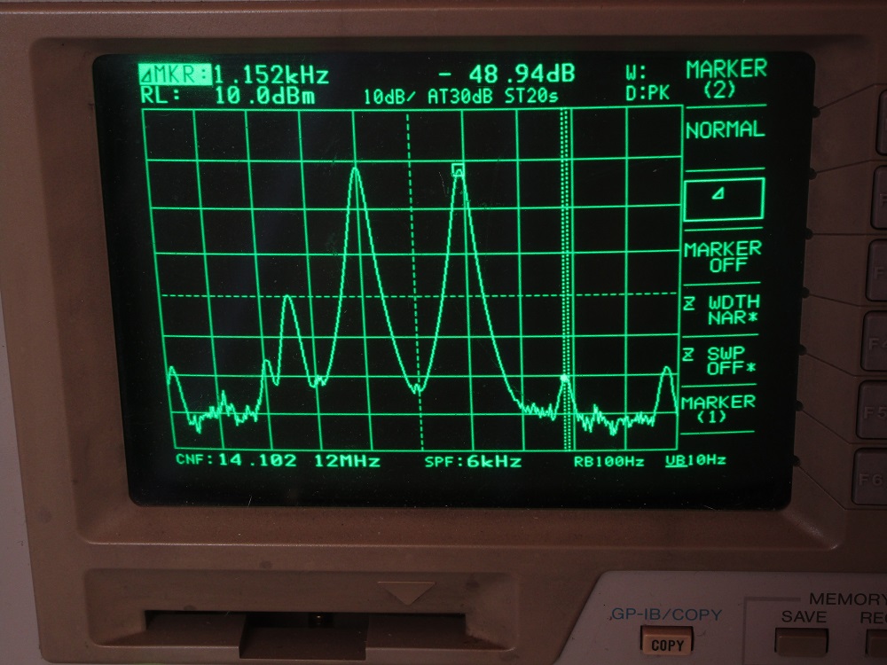
Here is the two tone test with 700 Hz and 1900 Hz tones. The peak power in this test is 100 watts. One the high side, there is an IMD3 product at -49 dBc
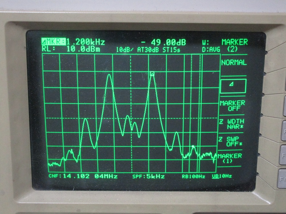
On the low side, the IMD3 product is at about -51 dBc
Notice that the two tone tests show the peaks are about 6 dB below that of a single tone?
The reason can seen in the time domain photo of the envelope of the two tone test posted earlier. The peaks are at 100 watts but the average power is about half. Then the power is split equally between the 700 Hz and 1900 Hz tones which reduces power by another 3 dB causing the drop of about 6 dB.
This 6 dB is what separates the ARRL method of measuring IMD from the method used here which is how far down the IMD product is relative to one of the two tones resulting in the nomenclature of dBc.
I suspect this helps dispel any notion that the PM2 power supply might degrade the IMD performance of the KWM-2.
Now for an examination of what those other products are and how to eliminate them.
I suspect they are mostly caused by the harmonics of the lower tone at 700 Hz since the second harmonic at 1400 Hz and the third at 2100 Hz will be within the mechanical filter bandwidth.
Below, I varied the output of the audio source while using the microphone gain control to maintain 100 watts at the output. The best I could do was to get the second harmonic down about -47 dBc.

As can been seen below, getting the second and third harmonic down improved the situation considerably.
I was a bit disappointed that the lower IMD3 came up.

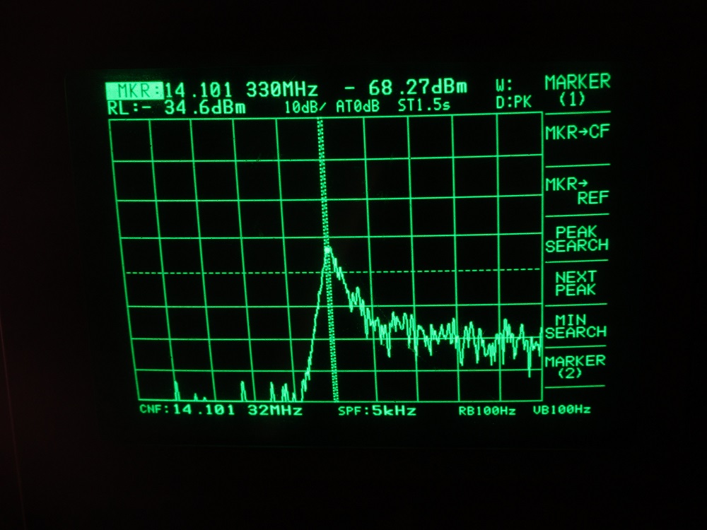
In the tests below, I used the test frequencies found in Collins test procedure for the KWM-2, 950 Hz and 2000 Hz initially. This has the advantage that the third harmonic of 950 Hz ( 2850 Hz ) will be cut off by the mechanical filter. I had to back down to 850 Hz because the lower IMD3 product was hidden by the carrier leakage.


I seem to have out of spec carrier leakage.
In the test below, I adjusted C120, the feedback neutralization capacitor, to see if it could minimize the IMD3 products further. There was a null that lowered IMD3 down to about -45 dBc not far from the original position of C120 after calibration.

The KWM-2 manual states that the carrier leakage to the output should be less than 0.2 Vrms which is 0.8 mW or about 0 dBm. I measure -28.77 dBm after a 45.32 dB of attenuation. So at the input of the attenuator, would be 45.32-28.77 = +16.55 dBm which is well above 0 dBm.
Some schematics show a quad ring for the balanced mixer but this is an older design with four 1N34A germanium diodes. The carrier balance involves using selected parts.
R15 and C9 are the mixer balance adjustments. C10 is a selected value. It was 27 pF. Circled in red are the four 1N34A’s.

After trying some selected values for C10 starting from the original 27 pF, 33 pF, 39 pF, 47 pF, 51 pF some success was achieved. The leakaged dropped from -28.77 dBm to about -37 dBm. Not sufficient to meet the -45 dBc specification.
The four 1N34A diodes were removed and tested using a Fluke 77 in diode test mode. The results are on the left. On the right are five randomly selected 1SS97 Schottky diodes I happen to have. As can be seen, even randomly picked 1SS97’s are very well matched compared to the 1N34A’s.
Replaced the 1N34A’s with the 1SS97’s. The carrier leakage is now about -53 dB below the 700 Hz tone.
In the paper posted by VK6HP, KC6BC says that carrier suppression can reach 50-70 dB. I had noticed that after achieving the factory specification of -45 dB, C9 in the photo below was at its minimum capacitance position with the notch circled in green pointing farthest away from the two mounting screws circled in red.

Under the chassis there is a factory selected 27 pF capacitor in shunt across C9. This was removed and replaced with a 10 pF capacitor. That allowed nulling the carrier down to -68 dBm at the output of the 43.3 dB attenuator. Since 4.68 dBm represents 100 watts after the same attenuator, -68 dBm below +4.68 dBm would be -72.68 dBc
With carrier leakage that low, the carrier vanished into the noise in the one tone ( 700 Hz ) output. Other than as an experiment, I do not recommend trying to hold carrier suppression at these levels. There is too much drift in the circuit. The suppression will wander up about 7-8 dB just over a short time.

The paper also suggests that the diodes forward bias voltage difference be held to 10 mV or less to meet the carrier suppression specification. Given that Collins tests carrier suppression, the original 1N34A diodes must have meet specification 60 years ago but now the forward voltage difference is closer to 100 mV. This is one of those rare instances where semi-conductor aging can affect a specification.
IMD further improvements
After solving carrier leakage problem, IMD3 had deteriorated to about -44 dBc. I decided to go back and revisit IMD testing to see if this could be improved back to the level of about -48 dBc. It took some time but KWM-2 can achieve -50 dBc IMD3 in a class AB amplifier. Like carrier leakage of -72 dBc, this is not easy to hold. It looks like a repeatable level for IMD3 is probably around -44 to -48 dBc.

The only rig I know of that can do better is the Yaesu FT1000MP MarkV which can achieve -55 dBc using a class A amplifier although it may be limited to 75 watts PEP.
I also calculated where the lower IMD3 product would be using 950 Hz and 2000 Hz as tones. It would be at 14.0999 kHz. The carrier leakage would be 100 Hz away at 14.1 kHz. Either Collins had a very good spectrum analyzer back in the late 50’s that could resolve signals separated by 100 Hz or they didn’t expect IMD3 to be equal to the carrier leakage but higher.
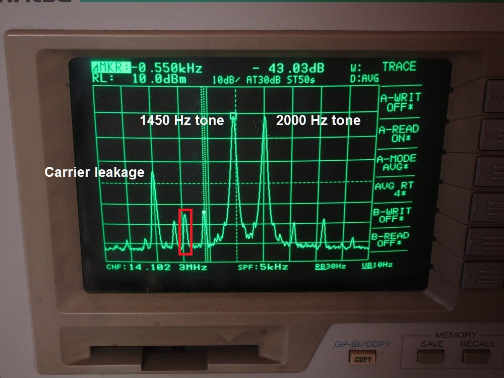
These are two tests using different tones to see if more undesired signals could be eliminated. 1450 Hz and 1600 Hz were used for the low tone because their harmonics would be removed by the mechanical filter.
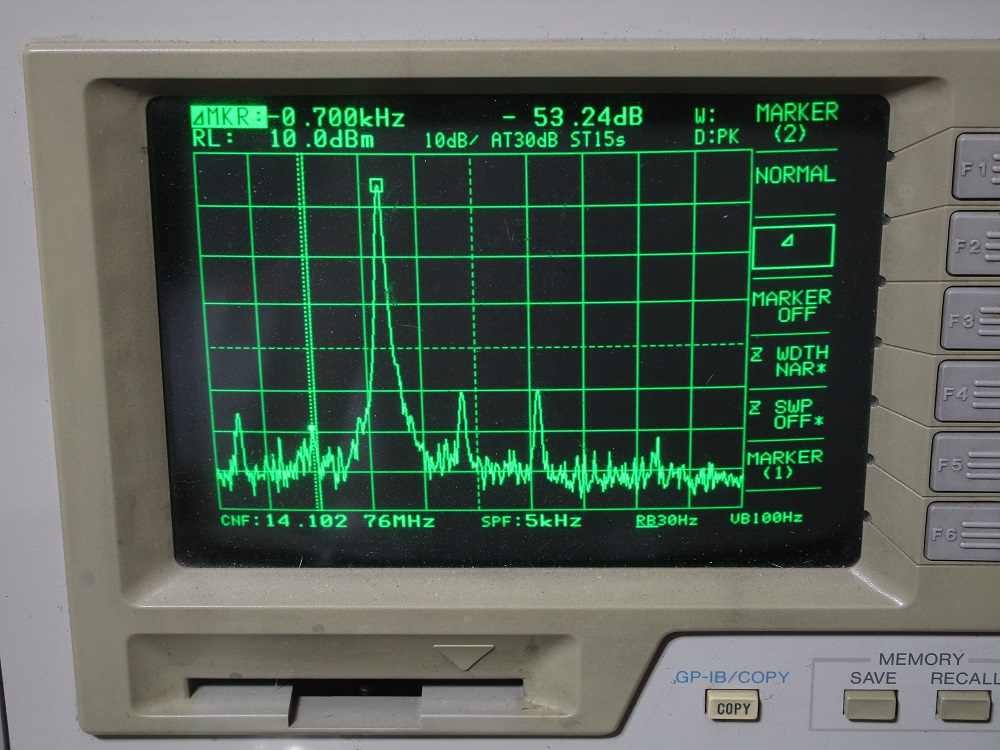
Tones at 1450 Hz and 2000 Hz. Circled in red is the largest unexplained spurious signal. It is suspected that it might be related to the carrier leakage.
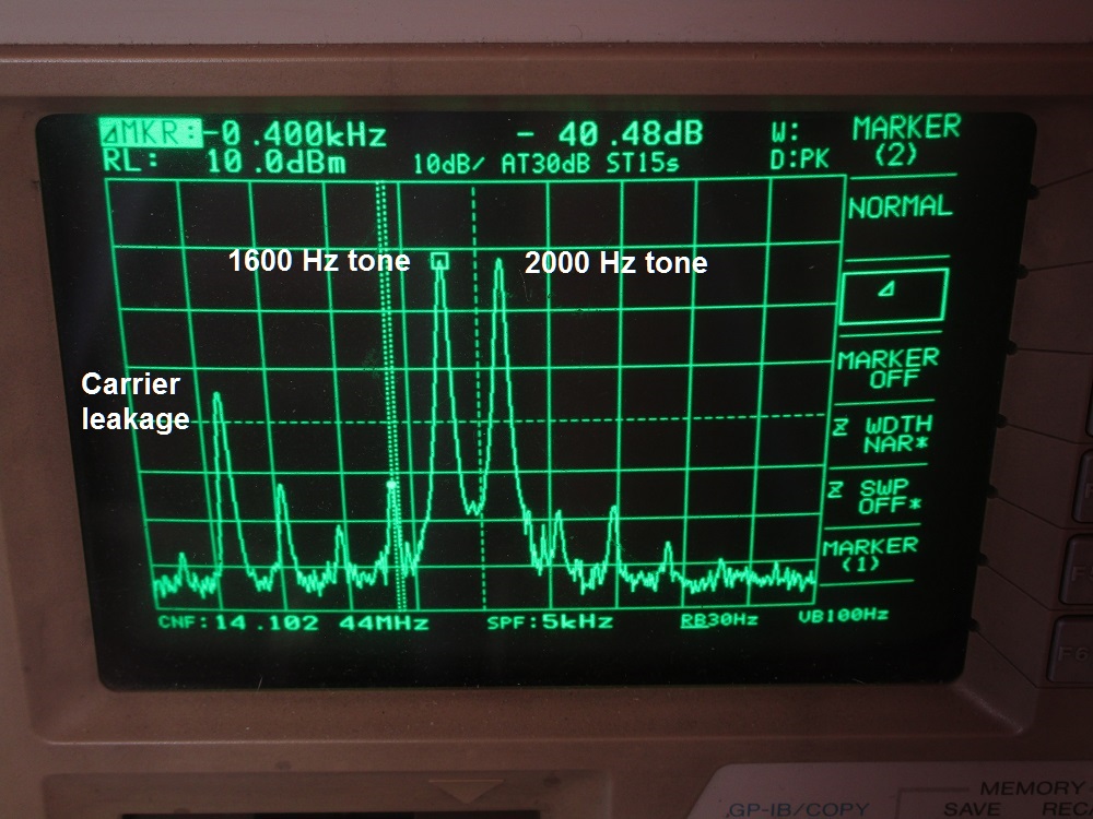
Tones at 1600 and 2000 Hz. Moving the carrier further away eliminated the above spurious.
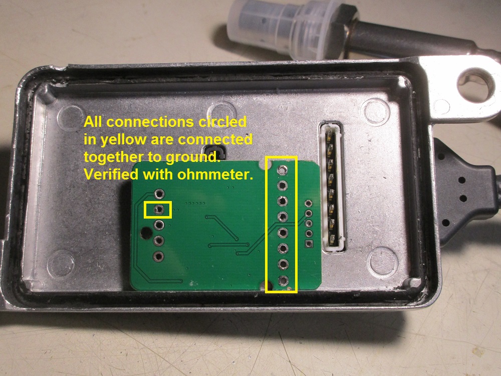
This sensor was recently purchased from an Aliexpress vendor who is not believed to be involved in this fraud. The vendor was also deceived by whomever is manufacturing these fake Nox sensors.
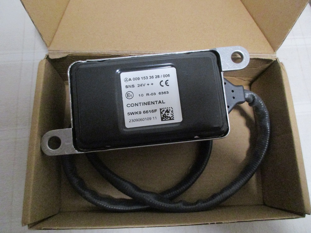

The giveaway was that a genuine Nox sensor has a heater to bring it to temperature. This part did not get warm. The cover is held in place with what appears to be black silicone just around the edges. The cover was popped off. This is what is inside.

The printed circuit board was un-soldered and flipped over. It can be seen that all the pins circled in yellow to the “sensor” are connected together and to ground.
This was not a restoration entered into lightly. I first saw that TS-830S after visiting a garage sale for a Lafayette HA600A receiver. The owner explained that the TS-830s had all the filters but there were many problems.
1.The 12BY7 socket might be loose.
2. 25 watts out on 10 m, 60- 90 watt on the other bands
3. The stator and rotor in the “load” capacitor seems loose
4. The received signal disappears if the tube heater are turned on unless in CW mode with the a key plugged in.
These were just the known problems with the possibility of more problems being hidden by these known one. The owner named a price but I declined at the time but bought the Lafayette receiver which had one known problem. The owner said he was taking to the next hamfest to sell or would part it out since he was aware of the prices the crystal filters were selling for on eBay. We left it at that.
Weeks later I had text message from the owner, that it had not gone to the hamfest. He was attempting to fix it himself. He asked for some advice which I gave him. In the mean time, I explained how his dad’s old Lafayette receiver issues had been resolved. Again there was discussion about parting the TS-830S for its filters.
In the meantime, I had learned that the TS-830S used Collins type feedback in its amplifier to reduce IMD. K1MH had posted
“Thats the basic test and you have to start with knowing the IMD of the xcvr
even if just doing a system test. I use a TS-830 with a measured -42 dB IM3
and that wont corrupt the amp reading as would something at -28 or so.”
I made a low offer for the TS-830S which I did not expect to be accepted. The owner went back to trying to service it himself. Again, weeks went by when a text message arrived that he was willing to accept my offer if it was still good. In the end, the owner could not bring himself to part out the TS-830S. He wanted it restored and in a good home as had happened with his dad’s Lafayette receiver.

The loose screw behind the “load” capacitor is circled in red. A jewelers screwdriver was used to tighten it without removal. Some Loctite was applied as well.

Full power on all bands was restored but it was not to last. After the TS-830S was turned off for about an hour, it turned back on with no output power.

Probing the 12BY7A tube socket, it was found that the plate voltage was missing. The RF Unit was removed and inspected. Pin 7 of the 12BY7A socket was found to be only partly soldered. Completing the job and re-installing the RF Unit now results in more stable output power.

This is an error analysis showing how the IMD3 of the source affects the accuracy of the IMD3 measurement of an amplifier with a gain of A dB.
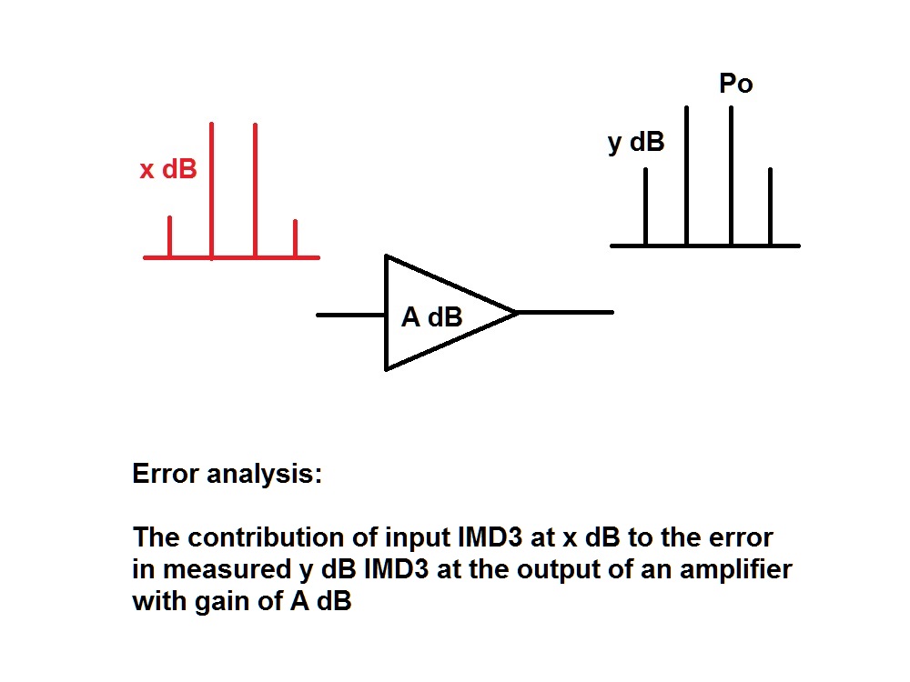
If the output power of the amplifier is known, Po, then Pin from the source is Pin = Po – A dB. If the IMD3 of the source is x dB below Pin, then it can be shown that the power of the IMD3 contribution of the source is simply Pin – x dB or ( Po – A dB ) – x dB. If the IMD3 power contribution of the source is amplified by A dB, the contribution of the x dB from the source at the output of the amplifier is ( Po – A dB ) – x dB + A dB = Po – x dB.
Let Pimd3s = the power of the IMD3 component of the source = ( Po – A dB ) – x dB
Let Pimd3a = the power of the IMD3 component of the amplifier = Po – y dB
The error in the Pimd3a is the amplified Pimd3s term.
So Pimd3a with its error term is Pimd3a +/- ( Pimd3s + A dB )
Let’s use a example where,
Po = 500 watts or 54 dBm
x = 37 dB
y = 24 dB
What is the error in the measurement of the y dB amplitude?
Using Pimd3a +/- ( Pimd3s + A dB )
Pimd3a = ( 54 dBm – 24 dB ) = 30 dBm = 1 watt = 1000 mW +/- ( Pimd3s + A dB ) = ( Po – A dB ) – x dB + A dB = ( Po – x dB )
1000 mW +/- ( 54 dBm – 37 dB ) = 17 dBm or 1000 mW +/- 50 mW or 950 to 1050 mW.
Expressed in dBm, 950 to 1050 mW is 29.777 dBm to 30.212 dBm or 30 dBm +0.21 dBm, – 0.223 dBm. This is the approximately 0.5 dB error VK6HP referred to earlier. This is the case where the source is 13 dB cleaner than the amplifier.
Let’s use an example where the source is only 10 dB cleaner than the amplifier all else the same.
Pimd3a = 1000 mW +/- ( 54 dBm – 34 dB ) = 20 dBm or 1000 mW +/- 100 mW or 900 mW to 1100 mW
Expressed in dBm, this would be 29.54 dBm to 30.41 dBm or 30 dBm +0.54 dBm, – 0.46 dBm. The total error just under 1 dB.
Let’s use an example where the source is 20 dB cleaner than the amplifier all else the same.
Pimd3a = 1000 mW +/- ( 54 dBm – 44 dB ) = 10 dBm or 1000 mW +/- 10 mW or 990 mW to 1010 mW
Expressed in dBm, this would be 29.956 dBm to 30.043 dBm or 30 dBm +0.043 dBm, – 0.044 dBm. The total error just under 0.1 dB.
The TS-830S does not have too many carbon composition resistors but there are a few like this 470k plate resistor for the 12BY7A. It’s p/n is RC05GF2H474J. The “J” representing +/-5% which means a 5% high value would be about 493K. Unfortunately, as with many aged carbon composition resistors this one is about 15% high.
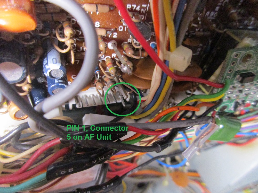
After replacing R38, the 470K carbon composition resistor in the plate circuit of the 12BY7A, and old problem came back. The bias to the finals vanished again. Before, I thought this to be due to dirty connectors but as can be seen in the photo below, the real problem was that a connector pin had become unsoldered from the printed circuit board. This pin is grounded by the relay on the AF Unit to reduce the negative grid bias so grid current can flow but as it had become unsoldered, the relay could not ground it in transmit mode.
To replace parts like R38, the plate resistor for the 12BY7A driver, on the RF Unit board, it is necessary to separate switches S1 and S22. S22 is the wafer switch consisting of three wafers inside the RF cage which selects the band components for the pi network output. This is a simple way to align its wafers to connect via the nylon coupler to the main bandswitch S1 after the two have been separated. The nanoVNA is inserted between ground of the RF cage and the plate cap of the 6146W that was removed. It shows the resonance of the pi-network established by switch S22 to be about 14 MHz which fortunately is where the bandswitch S1 is also set.

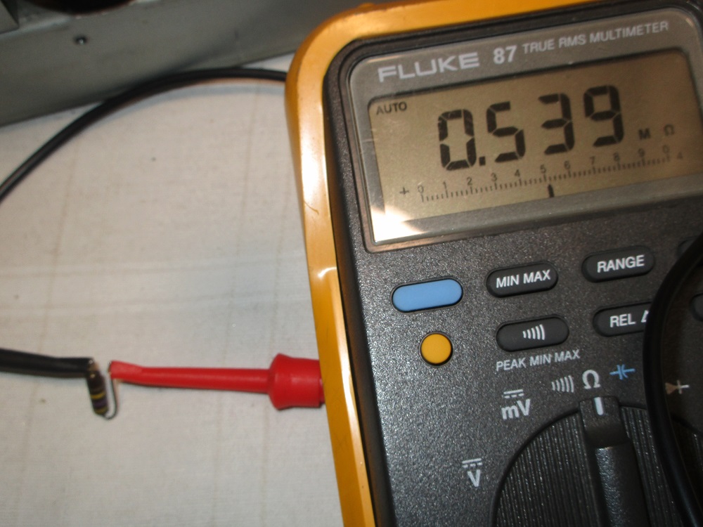
Testing the parasitic suppressors
The parasitic suppressors are a few turns of wire wrapped around a 47 ohm carbon composition resistor. An attempt was made to determine the value of the 47 ohm resistor without unwinding one end from the coil. The newer nanoVNA’s have the ability to interpret Smith chart data in either admittance or impedance format.

The admittance Smith chart was chosen to display Rp + L/C. This is the nanoVNA display. It shows that the 47 ohm resistor has been transformed to over 160 ohms. Let’s see how that happened.

This is the 47 ohm carbon composition resistor by itself showing some lead inductance.
This is the coil around the resistor.
The behavior of the suppressor is materially changed by the series inductance of the resistor represented by L2 and the length of wire used to attach it between the plate choke and plate cap represented by L3 as shown by the SimNEC analysis. Take the Y parameter real part of 6.94 m and invert it. The resistance is about 144 ohms.
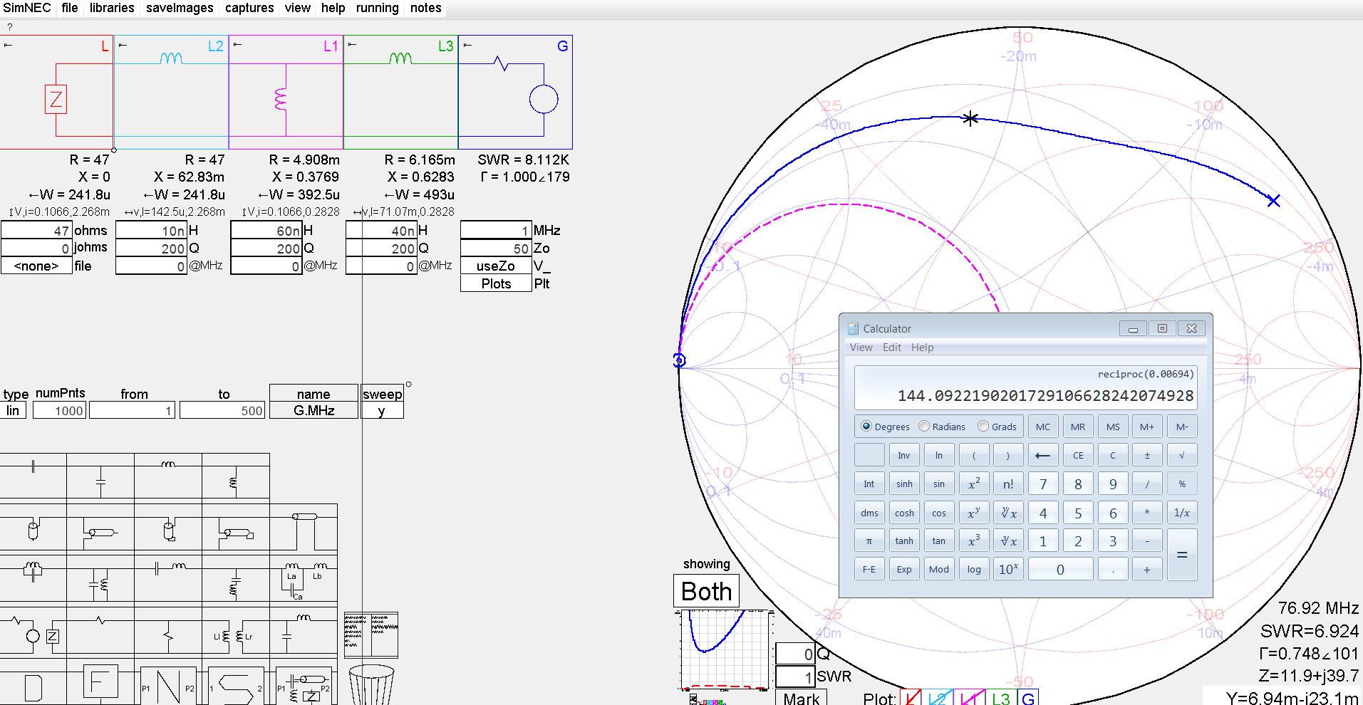
Once it was realized how strong the contribution of lead length is, the lead length in the test fixture was reduced to about 1 1/4″ with the result that resistance is reduced from about 162 ohms to 83 ohms. The length of the resistor body is 0.5″ which limits how short the leads can be.

Today I took out the final unit pcb to check the carbon composition resistors on it. The carbon composition resistors are labelled in red. Labeled in green are probably carbon film resistors.
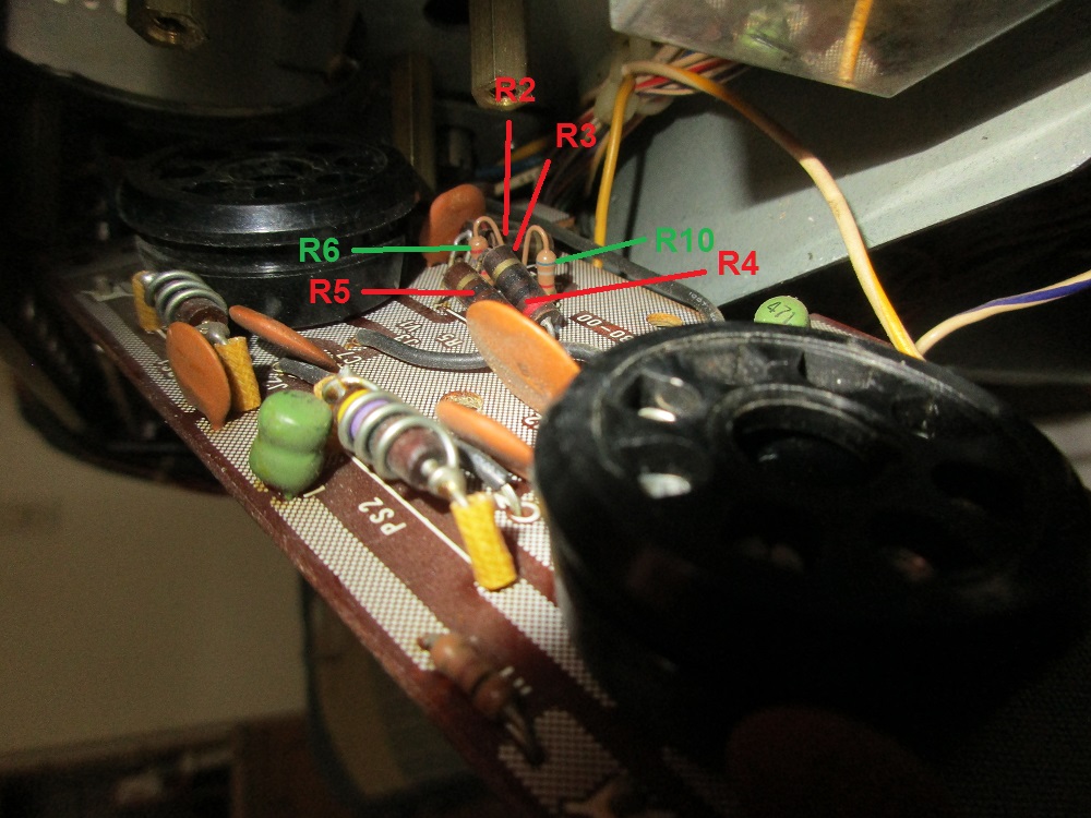
These are the actual measured values of the carbon composition resistors marked in red above. R10 has been changed from the 4.7k on the schematic to a 6.8k resistor.
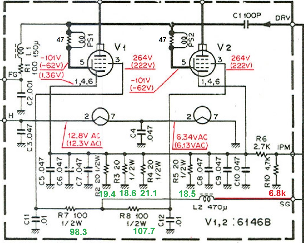
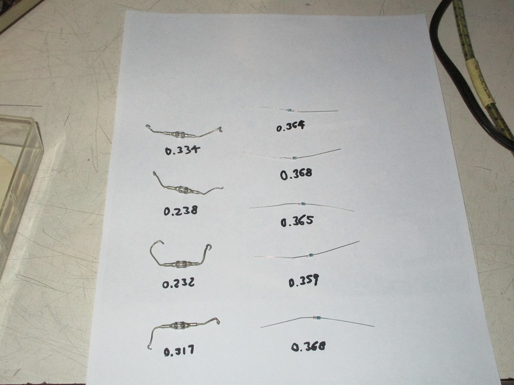
PS1 and PS2 are grid suppressors wound on 47 ohm carbon composition resistors used as a form. Both were scanned with a VNA.
This is PS1

and, PS2. No problems were found with the carbon composition resistors.

Before attempting alignment, it seemed prudent to check all the crystal and ceramic filters due to their age. I was particularly concerned that the ceramic filter might have suffered from degradation widely reported in TS2000.
These tests were done with a nanoVNA attached to the bare wires of the filter switching diodes with a 1000 pF capacitor and 1 K resistor in series with the probe.
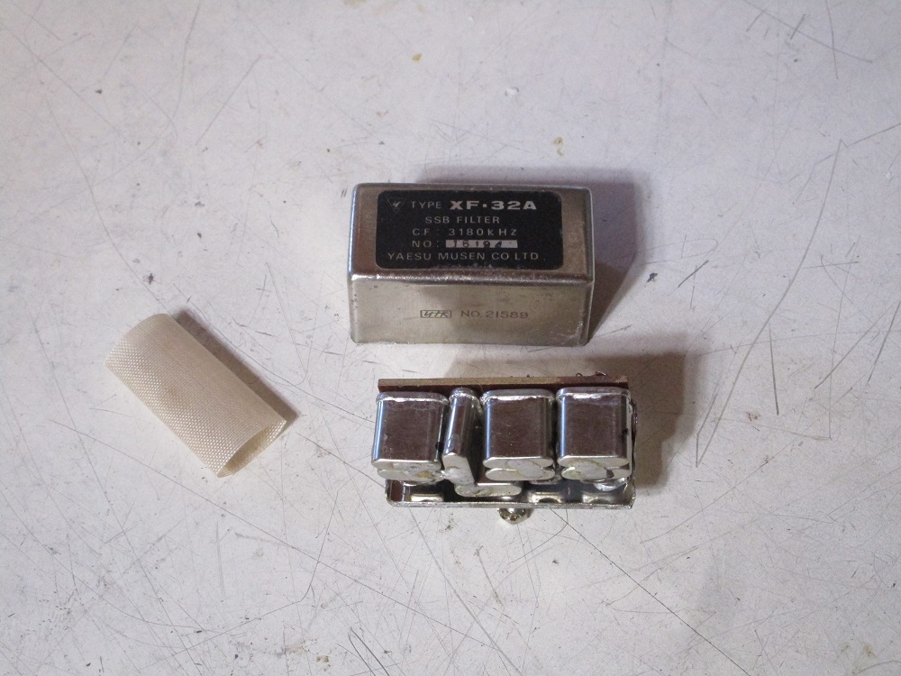
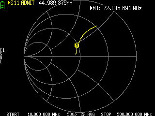
This is the 8.83 MHz SSB filter
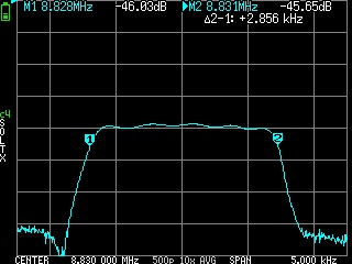
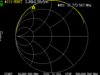
This is the 8.83 MHz 500 Hz CW filter. Actual specified center frequency is 8.83 MHz plus 700 Hz.

This is the 455 kHz SSB ceramic filter. The lumpiness is probably due to the input/out impedance of this filter being 2k so the nanoVNA with the 1k resistors is loading it significantly. The crystal filters have 600 ohm input/output impedances so are not loaded as much.

This is the 455 kHz 500 Hz CW filter. Actual center frequency is 455 kHz plus 700 Hz.
Fortunately, all the filters are behaving correctly.
The alignment of the VBT ( 8.375 MHz ), USB ( 8.8315 MHz ), and LSB ( 8.8285 MHz ) crystal oscillators was done as shown below. The antenna that came with the TinySA Ultra was poked into one of the holes in the bottom of the TS-830S. It could easily pickup all three oscillators. The alignment of the VBT oscillator required taking the top cover off since it is located near the rear panel on the IF assembly.
The bad news was that one day after the alignment was done, I came back to check the IF shift which is just observing how much the IF shift control can move the USB and LSB crystal oscillators, and found the VBT oscillator was 1.5 kHz low, and the USB, LSB oscillators were both about 700 Hz low.
I re-calibrated them, then checked the IF shift which was fine, but there may be an issue with the power supply for the tuning diodes for the three oscillators. Today I rechecked. The VBT and LSB oscillators were correct, the USB oscillator was about 100 Hz low.
Since the accuracy of the VBT, USB, and LSB crystal oscillators play such a great part in the performance of the TS-830S, I decided to spend time to understand a problem I have seen. The issue is not drift but what might be termed resettability. By this is meant, after calibration, the oscillators show no drift, but if the TS-830S is turned off for eight hours and turned back on, the oscillators are no longer at their set frequency. If this on/off cycle and test is done repeatedly, it was found that there was a random movement of the oscillators. For example, the VBT oscillator – no change, the LSB oscillator -100 Hz, the USB oscillator -125 Hz. Next cycle, the VBT oscillator is -100 Hz, the LSB and USB oscillators – no change.
I cleaned all the connectors on the PLL board. The VBT oscillator shows no drift but the LSB and USB oscillators shifted up about 50 Hz. Resetting them, they again moved up 50 Hz after a day. After watching for a few days, I found the drift does not accumulate. I then did the LSB and USB calibration by setting them 50 Hz below the proper frequency. The following day both had moved up 50 Hz to the proper frequency. I suspect that the adjustments capacitors for these two oscillators being away from the edge of the PLL board means the board may deflect during calibration causing an error once the board has sufficient time to go back to its natural rest position. The VBT oscillator adjustment is next to the rear edge of the IF board less than an inch from a screw that holds the board in place does not suffer this effect.
It looks like the connectors that supply the tuning voltages to the varactor on the PLL board play a significant role in the resettability problem.
IMD3 tests with tones at 1 kHz and 1.575 kHz are as used by Kenwood but I realized that Kenwood never says what the output power is when they did their measurement. Also, I was not able to get the carrier suppression as good as in the Kenwood ad plus there were other spurious that appears. The carrier is circled in yellow below. A 40 dB, 100 watt attenuator is being used at the output so 10 dBm on the spectrum analyzer screen represents 100 watts.
At 5 watts in each tone, the IMD3 is about -32 dBc.

At 1 watt out, the IMD3 is about -37 dBc
At about 0.3 watts out, the IMD3 is about -44 dBC.

The Kenwood TS-830S is one of the most ergonomic rigs I have ever owned. Unfortunately, since it was produced between roughly 1980 to 1988, the tune up procedure is pretty dated and rather cumbersome.
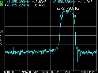
This weekend I spend some time looking into whether using modern tools, it is possible to avoid some of the old procedures and end up with a respectable frequency calibration.
The two tools used were a sweeping function generator and the Icom 705 with a small telescoping antenna borrowed from the TinySA Ultra spectrum analyzer. Any transceiver with a similar display should work. The 705 measurements are all done via the antenna so it never touches the TS-830A. The set up is shown below,

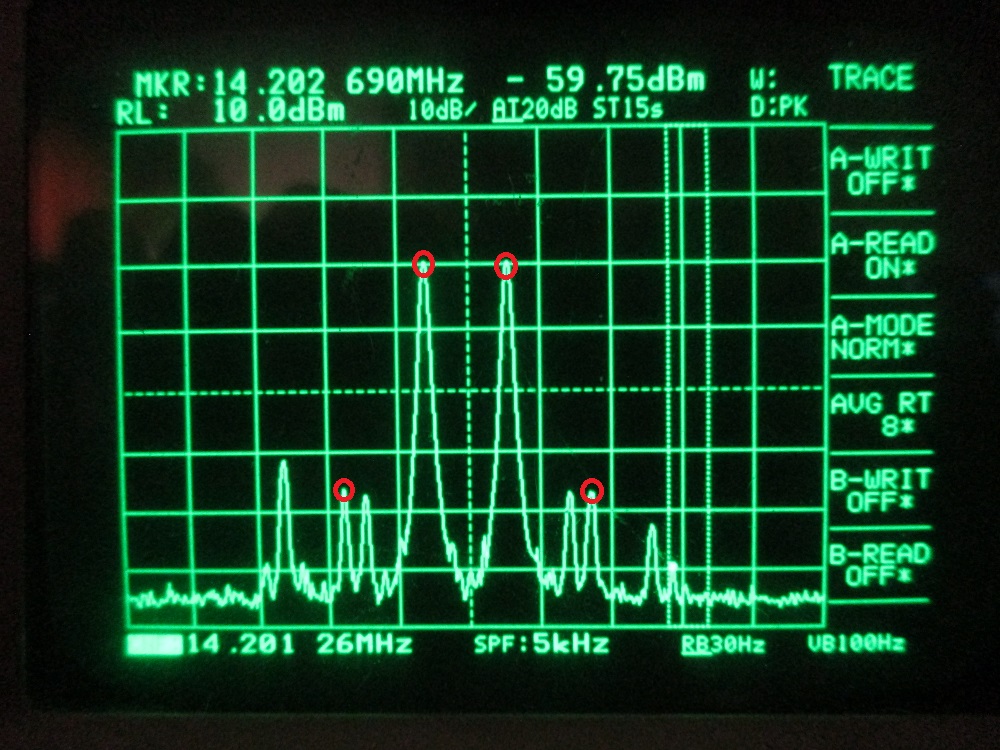
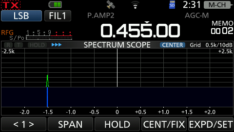
The Icom 705 is used to set the VBT oscillator for 8.375 MHz. The 705 was tuned to 8.376 MHz with a 5 kHz span so the 8.375 MHz VBT crystal oscillator signal is 1 kHz below the center frequency.

The LSB ( 8.8285 MHz ) and USB ( 8.8315 ) xtal oscillators were set by using the 705 tuned to 455 kHz. The LSB/USB crystal oscillators were then set to be 1.5 kHz about and below 455 kHz as shown in the 705 screen captures.

The final test was done by monitoring the output frequency with the 705 while using a function generator to sweep the microphone input from 300 Hz to 3 kHz. The 705 max hold function is used to store the sweeps so the actual SSB passband through the crystal or ceramic filters can been seen. It may look like an AM spectrum but is is actually composite image. The LSB and USB signals were scanned separately. The 705 peak hold stores both so they can easily be compared.

The sweeping function generator was simply a convenience. Any function or audio generator can be used by manually tuning the range desired. The peak hold function still provides a reasonable passband presentation. This particular TS-830S has the full complement of four filters so the passbands shown are though two SSB filters.